- SJ_Zhang
- Apr. 6, 2025
Abstract
All-perovskite tandem solar cells are promising as next-generation high-efficiency photovoltaic devices. However, further progress in tin-lead (Sn–Pb) mixed perovskites, which are essential as the narrow-bandgap bottom sub-cell, is hampered by unbalanced crystallization processes, leading to inhomogeneous films and reduced power conversion efficiency (PCE). Here we provide a complete understanding of the formation of Sn–Pb films, from the precursor solution to the final film. We find that the total crystallization barrier for Sn-based perovskites is limited by the desorption of dimethyl sulfoxide (DMSO), while Pb-based perovskites experience a smaller DMSO desorption barrier. By engineering the reaction barrier in mixed films via tailoring the DMSO content, we obtain synchronous Sn–Pb perovskite crystallization and high-quality homogeneous films. On the basis of this understanding, we demonstrate single-junction Sn–Pb perovskite solar cells with a PCE of 22.88% and all-perovskite tandem devices with a certified PCE of 28.87%, fabricated by antisolvent-free methods. The unencapsulated tandem devices retain 87% of their initial PCE after about 450 h with maximum power point tracking under 1 sun illumination.
Main
All-perovskite tandem solar cells (TSCs) have emerged as a promising photovoltaic technology owing to their high theoretical power conversion efficiency (PCE, >44%), low-temperature processing and low cost1,2,3,4,5,6. Recently, an impressive PCE of 30.1% was achieved, far exceeding the efficiency of all single-junction solar cells, showcasing its great potential7. Sn–Pb narrow-bandgap (NBG) perovskite bottom sub-cells, as a vital component of all-perovskite TSCs, play a key role in current matching and improving the PCE of all-perovskite TSCs8,9. Through previous great efforts, the PCE of Sn–Pb NBG perovskite solar cells (PSCs), based on the antisolvent-assisted method, has been improved to 23.8% through combinatorial optimization strategies such as Sn2+ oxidation suppression2,10,11 and defect passivation12,13,14,15. However, the PCE is still far behind the theoretical limit of ~33% and the efficiency of conventional-bandgap Pb-pure PSCs (26.15%)16. This inferior efficiency is attributed to the high defect density, greater film roughness and non-uniform element distribution of mixed Sn–Pb perovskite films, resulting from intrinsic Sn2+ oxidation and the unbalanced crystallization process of mixed Sn–Pb perovskites13,17,18,19,20.
In addition, the efficiency gap is particularly pronounced for both single-junction NBG PSCs (PCE of 21.4%) and all-perovskite TSCs (PCE of 26.8%) fabricated by antisolvent-free techniques (for example, vacuum- and gas-assisted methods)21, since the solvent extraction rate is nearly four orders of magnitude lower than with the antisolvent-assisted quenching strategy22, which would exaggerate phase separation and defect formation associated with the asynchronous crystallization between Sn- and Pb-based perovskites21,23. Nevertheless, antisolvent-free techniques are exclusively chosen by perovskite photovoltaic companies for mass manufacturing owing to their advantages for large-scale, high-repeatability, low-cost and environmentally friendly production4,21,24,25,26,27.
The different crystallization behaviour between Sn- and Pb-based perovskites was initially proposed by Prikas and colleagues in 199828. They revealed that SnI2 has a significantly higher reactivity with organic halides compared with PbI2 owing to its stronger Lewis acidity. Currently, this theory is widely used to guide the selection of additives and passivators for mixed Sn–Pb perovskites29,30,31. For example, formamidine sulfonic acid and guanidinium thiocyanate were explored to regulate the crystallization process, benefiting from their strong coordination between Lewis basic electron-donating groups such as S=O and SCN− and the Lewis acidic Sn2+ and Pb2+ (refs. 13,14). Although the simple application of Lewis acid-based theory has enabled certain successes, its current formulation remains incomplete and ambiguous, proficient in clarifying the dissolution process of both raw materials and additives but lacking in explanatory power concerning the crystallization process. A typical ambiguity is that Sn-based perovskite has greater solubility in dimethyl sulfoxide (DMSO) compared with Pb-based perovskite, but it also has a larger precipitation rate during the solvent extraction process32,33. In addition, several studies have shown that the reactivity of both Sn2+ and Pb2+ can be influenced by many factors such as the number of coordination bonds rather than only the Lewis acid-based property34,35,36. Hence, fundamental understanding and precise manipulation of the formation processes of mixed Sn–Pb perovskites are urgently required and crucial, but the current research is markedly deficient.
In this Article, we provide a fundamental understanding from precursor solution to perovskite film at the molecular level. By analysing the four formation processes of perovskite, including the dissolution of precursor raw materials, the generation of the intermediate phase by solvent extraction, the desorption of the coordinated solvent in the intermediate phase and the transition from the metastable phase to the final perovskite, we find that the desorption barrier of DMSO from the intermediate phases together with the transition barrier from the metastable to perovskite phase jointly determine the total crystallization barrier. We conclude that Sn-based perovskite undergoes only one desorption barrier of 2.12 eV from the intermediate to perovskite phase, while Pb-based perovskites undergo two barriers, including one small desorption barrier of 0.99 eV from the intermediate to metastable phase and another high transition barrier of ~1.86 eV from the metastable to perovskite phase. We further quantitatively manipulated the DMSO/[Pb + Sn] ratio to balance the crystallization barrier and enable the production of high-quality Sn–Pb NBG perovskite films. Finally, by applying a vacuum-assisted technique, we obtained a PCE of 22.88% for single-junction NBG solar cells and a certified PCE of 28.87% for all-perovskite TSCs.
Results and discussion
The crystallization process in Sn- and Pb-based perovskites
The evolution from precursor solution to final perovskite includes four stages (Supplementary Fig. 1): (1) the dissolution of the precursor raw materials (for example, PbI2 and SnI2), (2) the generation of the intermediate phase by free solvent extraction, (3) the desorption of the coordinated solvent in the intermediate phase and (4) the transition from the metastable phase to the final perovskite.
The perovskite precursor solution was prepared by dissolving PbI2, SnI2 and the organic halides in N,N-dimethylformamide (DMF) and DMSO mixed solvent. Because solution coordination states can easily be influenced by the basic crystallographic characteristics of materials, we checked the crystal structures of PbI2 and SnI2 (Supplementary Fig. 2). Both of them exhibit a two-dimensional layered structure37,38. In PbI2, all the Pb atoms are coordinated with six I atoms, forming edge-sharing PbI6 octahedron units (Fig. 1a). In contrast, SnI2 possesses Sn atoms with two types of coordination, where one-third of the Sn atoms are coordinated with six I atoms to form SnI6 octahedron units while two-thirds of the Sn atoms are coordinated with five I atoms to form SnI5 pentahedron units (Fig. 1b and Supplementary Fig. 3). SnI5 has one lone pair of electrons and is prone to coordinate more solvent molecules such as DMSO. These structural differences are expected to affect the precursor dissolution and the formation of the intermediate phase.
Fig. 1: The evolution routes of Sn- and Pb-based perovskites from the intermediate to perovskite phase.
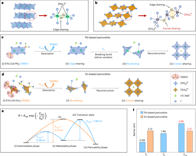
a,b, The crystal structure of PbI2 (a) and SnI2 (b). c,d, The evolution routes of Pb-based (c) and Sn-based (d) perovskites from the intermediate to perovskite phase. Stages i–iv represent the intermediate phase, metastable phase, transition state and perovskite phase, respectively. e, The desorption and transition barriers from the intermediate to perovskite phase. f, The desorption barrier E1, transition barrier E2 and total crystallization barrier Etot of Sn- and Pb-based perovskites.
Subsequently, the free solvent is removed by solvent extraction methods, and the intermediate phase forms (Fig. 1c–e, stage i). Clearly, both PbI2 and SnI2 are strongly coordinated by DMSO molecule at this stage. PbI2 is coordinated with one DMSO molecule, whereas we found that SnI2 coordinates with three DMSO molecules (Supplementary Figs. 4 and 5)35,39. The Sn–O bond length (2.18–2.32 Å; Supplementary Fig. 4) in the Sn-based intermediate phase is shorter than that of Pb–O in the Pb-based intermediate phase (2.49 Å)35. The higher coordination number and shorter coordination bond suggest that it is more difficult for DMSO to desorb from the Sn-based intermediate phase, which can also be further proved by the higher desorption temperature of DMSO in the Sn-based intermediate phase (154 °C versus 95 °C; Supplementary Fig. 5) and the downshift of the S=O stretching vibrational mode (Supplementary Fig. 6) compared with the Pb-based intermediate phase. Understandably, the generation rate from the intermediate phase should be strongly influenced by the desorption rate of DMSO, which can be described by the desorption barrier (E1; Fig. 1e) and the Arrhenius equation. We obtained the desorption rate at different temperatures on the basis of thermogravimetric analysis (TGA), as shown in Supplementary Text 1, fitted the desorption rate using the Arrhenius equation and obtained an E1 value of 2.12 eV and 0.99 eV for the Sn-and Pb-based intermediate phase (Supplementary Fig. 7), respectively. The E1 value of the Sn-based intermediate phase is 1.13 eV higher, indicating that DMSO desorption is more difficult, which echoes our previous analysis.
After DMSO desorption, the Pb(Sn)–I framework reacts with the organic halide to form perovskite, and we call the unreacted state the metastable phase (Fig. 1c–e, stage ii). This phase must undergo structural reorganization to establish a corner-sharing octahedral framework. For Pb-based perovskite, the metastable phase (Fig. 1c, stage ii) would inherit the edge-sharing feature of [PbI6]4− in the intermediated phase after DMSO desorption. Theoretically, the transition from edge-sharing units to a corner-sharing framework should include a Pb–I bond breakage process and a formation process for an isolated trigonal bipyramid (denoted as the transition state; Fig. 1c, stage iii)40. We define this transition barrier as E2. Subsequently, the free I− ions from the organic halide insert into the isolated [PbI5]3− to form a corner-sharing [PbI6]4− framework. Finally, the organic cations occupy the space enclosed by the [PbI6]4− framework to form the perovskite phase (Fig. 1c, stage iv). For Sn-based perovskites, the metastable phase (Fig. 1d, stage ii) inherits the no-sharing feature of [SnI5]3− in the intermediated phase. The no-sharing [SnI5]3− framework could spontaneously transfer into a corner-sharing [SnI6]4− framework through electrostatic attraction, and we believe that the barrier for this transition is negligible. Finally, the organic cations enter the corner-sharing [SnI6]4− framework to complete the perovskite phase (Fig. 1d, stage iv). Solid-state reactions reveal that SnI2·3DMSO and Cs0.2FA0.8I react immediately to form the perovskite phase once they come into contact at room temperature (Supplementary Fig. 8), confirming that the barrier for the transition from the no-sharing [SnI5]3− framework to the corner-sharing [SnI6]4− framework is negligible. Conclusively, the total crystallization barrier (Etot) for Sn-based perovskite is determined only by E1, while the Etot of Pb-based perovskite is determined by both E1 and E2, which accounts for the different crystallization rate in mixed Sn–Pb perovskite. Since the metastable phase is very difficult to harvest, we failed to measure E2 experimentally. We thus roughly evaluated E2 as the bonding energy of Pb–I (1.86 eV)41 because the formation of the transition state needs to break one Pb–I bond.
Clearly, the formation rates of Sn- and Pb-based perovskites depend on the collective rates of both DMSO desorption and phase transition from the metastable to perovskite phase. The total formation rate Rtot can be expressed by the Arrhenius equation as42

where Atot is the pre-exponential factor, kB is the Boltzmann constant and T is the absolute temperature. The Etot values for Sn- and Pb-based perovskites are E1 (2.12 eV) and E1 + E2 (2.85 eV; Fig. 1f), respectively. Therefore, for Pb-based perovskite, significantly more energy is required to overcome Etot, resulting in a much slower crystallization rate compared with Sn-based perovskites. Conclusively, maintaining nearly identical Etot values for the Sn- and Pb-based perovskites is the key to achieving synchronous crystallization.
Crystallization barrier control for synchronized growth
The vacuum-assisted method, one of the most promising techniques for future mass production of perovskite photovoltaics, was applied for the deposition of Sn–Pb mixed NBG PSCs. To achieve fast nucleation and a compact film, the vacuum should be as low as possible, and a threshold pumping time of 20 s is required to fully dry our film under a vacuum degree of ~3 Pa (Supplementary Figs. 9 and 10). The Sn–Pb mixed perovskite composition in this study is Cs0.1FA0.6MA0.3Pb0.5Sn0.5I3, which has an optimal bandgap of 1.22 eV for the bottom sub-cell15.
To obtain a uniform Sn–Pb mixed perovskite, we managed to fine-tune the Etot value to guarantee a balanced crystallization rate. Since the E2 value of the Pb-based perovskite relies on intrinsic atomic rearrangement and would stay relatively constant, we sought to tune the E1 value to balance Etot. Here, instead of additives, we simply set a series of ratios of DMSO/[Pb + Sn] to tune the coordination of Sn2+ and Pb2+ with DMSO and target synchronous crystallization (Supplementary Figs. 11 and 12). According to the above-mentioned method and Supplementary Text 1, we obtained the E1 value of the Sn- and Pb-based perovskites as a function of DMSO/[Pb + Sn] with a fixed Sn:Pb ratio of 1:1 (Fig. 2a). Both of them exhibited the nature of a smoothed step function. In mixed Sn–Pb perovskite precursor, because the coordination ability of Sn2+ is much larger than that of Pb2+, when the DMSO/[Pb + Sn] ratio is 1.5:1, all the Sn2+ should be preferentially coordinated with DMSO while the Pb2+ is at most partially coordinated with DMSO; when this ratio is 2:1, both Sn2+ and Pb2+ are prone to be exactly coordinated by DMSO (simplified as SnI2·3DMSO and PbI2·1DMSO). When the ratio is increased further to beyond 2:1, both Sn2+ and Pb2+ are in principle fully coordinated and free DMSO exists in solution. On the basis of the morphology, crystallinity and photoluminescence characterization, it is observed that the film quality initially improves but then deteriorates with increasing DMSO content (Supplementary Figs. 13 and 14). The film quality is optimal when Sn2+ is fully coordinated and Pb2+ is partially coordinated.
Fig. 2: Balancing the crystallization barrier of Sn- and Pb-based perovskites via precisely tuning the DMSO/[Pb + Sn] ratio.
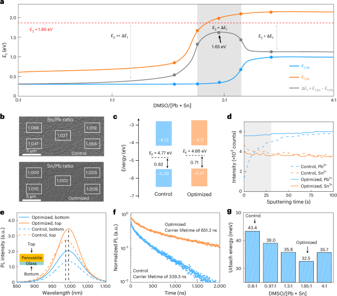
a, The desorption barrier E1 of Sn- and Pb-based perovskites as a function of DMSO/[Pb + Sn]. In the grey region, ΔE1 is close to E2, nearly balancing the crystallization rate for Sn- and Pb-based perovskites. b, The Sn/Pb ratio of the control and optimized perovskite films measured by energy-dispersive spectroscopy. c, Energy-level schemes of control and optimized perovskite films based on the ultraviolet photoelectron spectroscopy (UPS) spectra. d, ToF-SIMS of control and optimized perovskite films. The grey region denotes the upper surface of the perovskite film. e, Steady-state PL spectra of the control and optimized films excited from the top and bottom surfaces. f, Time-resolved photoluminescence spectra of control and optimized Sn–Pb perovskite films deposited on bare glass. g, The Urbach energy Eu of Sn–Pb NBG perovskite films extracted from absorbance spectra.
We then sought to identify the optimal crystallization window. The dashed red line denotes the reference line of E2, and the optimal processing window lies where E1,Sn − E1,Pb (denoted as ΔE1; Fig. 2a, solid grey line) is close to E2, thus enabling a nearly identical Etot. The grey region meets our requirements, where the DMSO/[Pb + Sn] ratio ranges from approximately 1.76 to 2.15. In this region, ΔE1 can reach 1.65 eV, which is very close to E2 (~1.86 eV). Thus, a synchronous crystallization rate is expected. We fabricated a series of solar cells with DMSO/[Pb + Sn] ratio ranging from 1.56:1 to 2.35:1 with ethylenediammonium diiodide (EDAI2) treatment. The difference in film thickness was relatively small, with a maximum variation of 80 nm (Supplementary Fig. 15), which is unlikely to affect device performance significantly15,43. According to the PCEs of these solar cells, we found that the optimal ratio window ranges from 1.85:1 to 2.05:1 (Supplementary Fig. 16). We also fabricated devices without EDAI2 and found that the optimal DMSO/[Pb + Sn] ratio remains the same (Supplementary Fig. 17), while EDAI2 treatment primarily enhances the device fill factor (FF)20 (Supplementary Fig. 18). Furthermore, the device PCEs with a DMSO/[Pb + Sn] ratio of 1.95:1 exhibited the highest efficiency with the smallest standard deviation. We thus chose this optimal device to compare with a control device fabricated with a ratio of 0.8:1 (a common ratio used in literature for antisolvent-free methods)4,25,44.
Characterization of mixed Sn–Pb perovskite films
We expect our optimized film to enjoy better composition uniformity and higher film quality thanks to the synchronous formation of Sn- and Pb-based perovskites. The horizontal Sn/Pb ratio revealed significant variation in the control film, while the optimized film exhibited a more uniform lateral Sn/Pb ratio, approximately equal to 1 (Fig. 2b). This indicates a more uniform elemental distribution in the optimized film, in accordance with surface potential results (Supplementary Fig. 19). We further observed an upwards shift in the Fermi level in the optimized film (Fig. 2c and Supplementary Fig. 20), indicating a more intrinsic film. We further evaluated the longitudinal homogeneity of Sn and Pb elements in mixed Sn–Pb perovskite films by using time-of-flight secondary-ion mass spectrometry (ToF-SIMS). For the control film, the Sn element was enriched on the surface while the Pb element gradually increased from the surface towards the bulk (Fig. 2d and Supplementary Fig. 21). This originates from the faster formation rate of Sn-based perovskite because, in our vacuum-assisted film fabrication, perovskite crystallization starts from the surface. For the optimized film, both Sn and Pb elements exhibit uniform distribution without much variation. The improved longitudinal homogeneity was also well confirmed by the identical photoluminescence emission peaks of perovskite film when excited from the top and bottom surface (Fig. 2e). As a result, the optimized film exhibited better uniformity thanks to the synchronous crystallization.
We further performed time-resolved photoluminescence to investigate the carrier dynamics in the films (Fig. 2f). The optimized perovskite film showed an average carrier lifetime that was twice as long (651.2 ns) as that of the control film (339.3 ns), indicating a reduced defect density. The Urbach energy (Eu) of the optimized films decreases from 43.4 ± 0.3 to 32.5 ± 0.26 meV (Fig. 2g), implying reduced structural disorder or secondary phases in the optimized film. We also found that the oxidation of Sn2+ was partly reduced in the optimized films owing to the reduced Sn element at the surface (Supplementary Fig. 22), which is also in line with the higher average surface potential and lower defect density near the surface for the optimized film compared with the control film (Fig. 2c and Supplementary Fig. 23).
Photovoltaic characteristics of Sn–Pb NBG PSCs
We then fabricated Sn–Pb NBG PSCs using the control and optimized perovskite films. The device structure was indium tin oxide (ITO)/poly(3,4-ethylenedioxythiophene):poly(styrene sulfonate) (PEDOT:PSS)/perovskite/C60/bathocuproine (BCP)/Ag, where the thickness of the perovskite layer is ~1,000 nm (Supplementary Fig. 24). Compared with control devices, the optimized devices showed improved performance across all photovoltaic parameters (Fig. 3a). The best-performing device has an open-circuit voltage (VOC) of 0.885 (0.871) V, a short-circuit current density (JSC) of 32.4 (32.5) mA cm−2 and a FF of 79.8% (78.2%), yielding a PCE of 22.88% (22.14%) under reverse (forward) voltage scanning (Fig. 3b), which is much better than the control devices (Supplementary Fig. 25 and Supplementary Table 1). The device PCEs with a narrow distribution are shown in Supplementary Fig. 26. The steady-state power output (SPO) efficiency of the device at the maximum power point is 22.53% (Supplementary Fig. 27). The integrated JSC values derived from the external quantum efficiency (EQE) curves of the control and optimized cells were 28.66 mA cm−2 and 31.98 mA cm−2 (Fig. 3c), respectively. The main EQE improvement stems from photons beyond 700 nm, which have a deeper penetration depth and are absorbed by the whole bulk film down to the perovskite–C60 interface. Thanks to the more homogeneous composition and reduced Sn4+-associated defects, these photogenerated carriers enjoy better collection in the optimized device, leading to the better EQE. Transient photovoltage characterization reveals that the decay lifetime of the optimized device (283 μs) is longer than that of the control device (44 μs; Fig. 3d), indicating that the carrier trapping and non-radiative recombination was substantially suppressed, which can also be further confirmed by the light intensity-dependent photovoltage (Supplementary Fig. 28). In summary, we demonstrate a PCE that compares favourably with reported antisolvent-free NBG PSCs (Fig. 3e and Supplementary Table 2). We further prepared Sn–Pb mixed perovskite films and devices using both gas-assisted and antisolvent methods. At a DMSO/[Pb + Sn] ratio of about 1.95:1, these films showed the highest crystallinity, and the corresponding devices show the best performance (Supplementary Figs. 29 and 30), demonstrating that this optimal DMSO range is effective for both antisolvent-free and antisolvent methods. In addition, this finding is also applicable to Sn–Pb mixed PSCs fabricated by both spin-coating and blade-coating methods (Supplementary Figs. 31 and 32).
Fig. 3: Device performance of optimized Sn–Pb NBG PSCs.
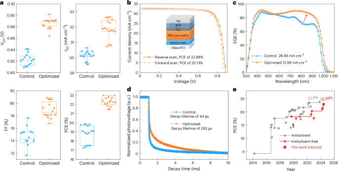
a, A comparison of the photovoltaic performance between control and optimized devices (16 individual devices of each type). The box represents the interquartile range (25–75th percentile) of the dataset, with the central line indicating the median value. Whiskers extend to 1.5 times the interquartile range. b, Current density–voltage (J–V) curves of the best-performing Sn–Pb NBG PSCs. c, EQE spectra of control and optimized Sn–Pb NBG PSCs. d, Transient photovoltage decay curves of control and optimized Sn–Pb NBG PSCs. e, A summary of reported PCEs of Sn–Pb NBG PSCs fabricated by antisolvent and antisolvent-free methods.
Vacuum-assisted all-perovskite TSCs
We then fabricated two-terminal all-perovskite TSCs. The top cell has an absorber composition of DMA0.1Cs0.4FA0.5Pb(I0.75Br0.25)3 (DMA = dimethylammonium; FA = formamidinum) with 5 mol% methylammonium lead chloride (MAPbCl3) additive. Detailed information about the wide-bandgap (WBG) top cells can be found in the Supplementary Information (Supplementary Fig. 33 and Supplementary Table 3). The tandem devices have a structure of glass/ITO/NiO/4PADCB/DMA0.1Cs0.4FA0.5Pb(I0.75Br0.25)3/C60/SnO2/Au/PEDOT:PSS/Cs0.1FA0.6MA0.3Pb0.5Sn0.5I3/C60/BCP/Ag, where 4PADCB is a self-assembled monolayer (4-(7H-dibenzo[c,g]carbazol-7-yl)butyl)phosphonic acid (Fig. 4a,b). Ultimately, our best-performing device showed a PCE of 28.95% (28.47%) under reverse (forward) voltage scanning, with a VOC of 2.134 (2.125) V, a JSC of 16.05 (16.03) mA cm−2 and a FF of 84.52% (83.58%). An independent laboratory also certified comparable efficiencies of 28.87% and 28.18% with reverse and forward voltage scanning, respectively (Fig. 4b, Supplementary Fig. 34 and Supplementary Table 4). The integrated JSC values of the WBG and NBG sub-cells obtained from the EQE spectra (Fig. 4c) are 16.01 and 15.96 mA cm−2, respectively, in good agreement with the JSC values determined from current density–voltage (J–V) measurements. We report a high PCE for all-perovskite TSCs fabricated by antisolvent-free techniques, including vacuum-, gas- and radiation-assisted methods and two-step methods (Fig. 4d and Supplementary Table 4). The device demonstrated an SPO efficiency of 28.53% at the maximum power point (Fig. 4e). We further fabricated 1.02 cm2 monolithic all-perovskite TSCs, which yielded a VOC of 2.09 (2.08) V, a JSC of 15.90 (15.83) mA cm−2 and an FF of 81.29% (80.84%), corresponding to a PCE of 27.01% (26.62%) under reverse (forward) scanning (Supplementary Fig. 35). The unencapsulated TSC retained 87% of its original PCE after about 450 h of MPP tracking (Fig. 4f), which is comparable to previous reports4,8,9. When operated at 65 °C, the tandem device maintained 60% of its initial PCE after 100 h of illumination (Supplementary Fig. 36), which is inferior to previous reports13,45. We attribute the low operational stability to Ag diffusion from electrode to perovskite, the volatile MA composition in NBG perovskites and the unstable PEDOT:PSS hole transport layer. Thus, we suggest several potential perspectives to improve the device stability, including replacement of the BCP with a compact SnO2 fabricated by atomic layer deposition (ALD), replacement of the PEDOT:PSS with an inorganic hole transporting layer such as NiO and the development of an MA-free NBG perovskite system.
Fig. 4: Device performance of all-perovskite TSCs.
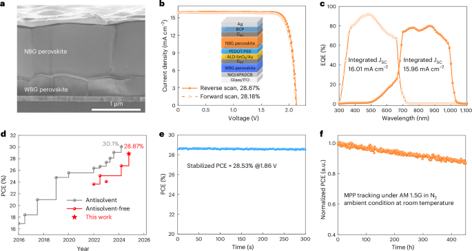
a, A cross-sectional scanning electron microscopy image of a representative tandem device. b, J–V curves of the tandem TSC certified by Shanghai Institute of Microsystem and Information Technology. c, The EQE spectra of the bottom and top sub-cells. d, A summary of typical PCEs of all-perovskite TSCs fabricated by antisolvent and antisolvent-free methods. e, The SPO of a high-efficiency tandem TSC. f, Continuous maximum power point (MPP) tracking of an unencapsulated tandem device.
Conclusion
We uncovered the formation pathway of Sn- and Pb-based perovskites, engineered the DMSO/[Pb + Sn] ratio to balance the crystallization process, obtained a mixed Sn–Pb NBG perovskite film with high uniformity and low defects and finally achieved a PCE of 22.88% for Sn–Pb PSCs and a certified PCE of 28.87% for all-perovskite TSCs obtained via an antisolvent-free method. Although some key findings have been revealed, the evolution from SnI2/PbI2 precursors to the final Sn–Pb NBG perovskite is very complex and many details remain elusive. More experimental studies as well as theoretical simulations should be carried out to fully understand the impact of surrounding organic halides, the exact transition barrier from the metastable to perovskite phase, the influence of temperature and concentration and so on. Nonetheless, our understanding could guide further optimization of Sn–Pb NBG perovskites with better homogeneity, less defects and thicker film, and lead to all-perovskite TSCs with >30% efficiency.
Methods
Materials
The raw materials were not subjected to any purification and were used as received. PbI2 (99.999%), SnI2 (99.999%), PbBr2 (99.99%), phenethylammonium iodide (PEAI) (99.5%) and NiO nanocrystal (99.999%) were purchased from Advanced Election Technology Co., Ltd. Formamidinium iodide (FAI) (99.5%), methylammonium iodide (MAI) (99.5%), methylammonium chloride (MACl) (99.5%), Pb(SCN)2 (99.5%), formamidinium bromide (FABr) (99.5%), CsBr (99.9%), CsI (99.999%), PbCl2 (99.9%), dimethylammonium iodide (DMAI) (99.5%), ethylenediammonium diiodide (EDAI2) (99.5%), propyldiammonium diiodide (PDADI) (99.5%), PEDOT:PSS, C60 and [6,6]-phenyl-C61-butyric acid methyl ester (PC61BM) were purchased from Xi’an Yuri Solar Co., Ltd. SnF2 (99%) was purchased from Aladdin Co., Ltd. 4PADCB was purchased from Vizuchem Co., Ltd. (Shanghai, China). Bathocuproine (BCP) was purchased from TCI. Tin powder (99.999%), N,N-dimethylformamide (DMF, 99.8%), dimethyl sulfoxide (DMSO, 99.9%), chlorobenzene (CB, 99.9%) and isopropanol (IPA, 99.5%) were purchased from Sigma Aldrich.
NBG perovskite precursor preparation
The mixed Cs0.1FA0.6MA0.3Sn0.5Pb0.5I3 NBG perovskite precursor with a concentration of 1.8 mol l−1 was prepared by mixing CsI (46.8 mg, 0.180 mmol), FAI (185.7 mg, 1.08 mmol), MAI (85.8 mg, 0.540 mmol), SnI2 (335.3 mg, 0.900 mmol), PbI2 (414.9 mg, 0.900 mmol), SnF2 (14.1 mg, 0.090 mmol) and Pb(SCN)2 (2.7 mg, 0.036 mmol) in mixed solvents of 0.25 mL DMSO and 0.75 mL DMF.
WBG perovskite precursor preparation
The WBG perovskite precursor with a concentration of 1 mol l−1 was prepared by mixing CsBr (42.56 mg), FABr (31.24 mg), DMAI (17.30 mg), MACl (3.38 mg), Pb(SCN)2 (3.25 mg), PbCl2 (13.90 mg), PEAI (2.5 mg), FAI (42.99 mg), CsI (51.99 mg), PbBr2 (55.05 mg) and PbI2 (391.85 mg) in mixed solvent of 0.2 mL DMSO and 0.8 mL DMF. The precursor solution was filtered through a 0.22 μm polytetrafluoroethylene (PTFE) filter before using.
NBG PSC fabrication
The pre-patterned ITO substrates underwent a cleaning process involving ultrasonication in deionized water, isopropanol and ethanol for 30 min in succession. PEDOT:PSS, which was diluted by n-propyl alcohol (1:5), was coated on the cleaned ITO substrate at 2,000 rpm for 30 s and then heated at 130 °C for 20 min. After cooling, the substrates were transferred to an N2-filled glovebox quickly, and perovskite films were spin-coated onto the substrate at 3,500 rpm for 8 s. The wet films were then directly transferred into a vacuum chamber (120 ml). After the vacuum pump was turned on, the vacuum level dropped to 3 Pa within 4–5 s. This high pumping rate enables us to prepare high-quality Sn–Pb perovskite films even with a high DMSO content. The total vacuum quenching time exceeded 20 s, including the pumping-down duration (Supplementary Fig. 9). Subsequently, the perovskite thin films were annealed at 100 °C for 10 min. After cooling, the perovskite films were post-treated by spinning a solution of EDAI2 (0.5 mg ml−1) in 1:1 IPA:CB solvent at 4,000 rpm for 20 s, followed by heating at 100 °C for 5 min. After cooling down to room temperature, 20 nm C60 film and 7 nm BCP were subsequently deposited by thermal evaporation at a deposition rate of 0.15 Å s−1. Finally, a 150 nm Ag electrode was deposited by thermal evaporation at a deposition rate of 0.5 Å s−1.
All-perovskite TSC fabrication
NiO nanocrystal dissolved in deionized water (4 mg ml−1) was spin-coated onto the ITO substrates at 5,000 rpm for 30 s, followed by an annealing process at 150 °C for 10 min. After cooling, oxygen plasma was used to treat the substrate for 5 min, then the self-assembled 4PADCB monolayer dissolved in ethanol (0.5 mg ml−1) was spin-coated onto the substrates at 3,000 rpm for 30 s, followed by heating at 100 °C for 10 min. After cooling, 45 µl of WBG perovskite precursor was dropped onto the substrate and spin-coated through a two-step process: 1,000 rpm for 5 s and 4,500 rpm for 40 s. At the 20th second, hot gas flow (70 m s−1, 50 °C) started, and the gas flow was maintained for 4–6 s, resulting in the film turning dark brown. After gas purging, the samples were annealed at 100 °C for 10 min. After cooling to room temperature, the perovskite films were post-treated by spinning PDAI2 solution (1 mg ml−1 in 1:1 IPA:toluene) at 5,000 rpm for 30 s, followed by heating at 80 °C for 5 min. Then, 20 nm C60 was deposited on top of the perovskite films by thermal evaporation at a rate of 0.15 Å s−1. The samples were then transferred to an atomic layer deposition system to deposit 30 nm SnO2. After that, 1 nm Au was thermally evaporated. After that, NBG sub-cells were fabricated using the above-mentioned methods.
Device characterization
The J–V characteristics were measured by using a Keithley 2450 sourcemeter and a solar simulator (EnliTech, class AAA, AM 1.5G). The AM 1.5G was calibrated with National Renewable Energy Laboratory reference solar cells (KG-5 and KG-0 reference cells were used). The bias voltage for J–V measurements of single-junction NBG PSCs was scanned from −0.1 V to 1 V (forward scanning) and from 1 V to −0.1 V (reverse scanning) with a scanning step of 0.05 V. The active area was determined by using aperture shade masks (3.95 mm2) placed in front of the solar cells. The bias voltage for J–V measurements of tandem cells was scanned from −0.1 V to 2.2 V (forward scanning) and from 2.2 V to −0.1 V (reverse scanning) with a scanning step of 0.05 V. The EQE measurements were performed in ambient air using a QE system (EnliTech) with monochromatic light focused onto a device pixel and a chopper frequency of 20 Hz. For the EQE measurements of TSCs, two light-emitting diodes with emission wavelength of 450 nm and 850 nm were used as bias illumination to measure NBG and WBG sub-cells, respectively. The operational stability was evaluated under multi-colour light-emitting diode illumination in N2. No UV filter was used during the stability tests. To assess the operational stability of the TSCs, we kept devices at a temperature of ~65 °C in N2 and measured their performance under simulated 1-sun illumination (a multi-colour light-emitting diode solar simulator with a spectrum profile equivalent to 100 mW cm−2).
Steady-state and time-resolved PL
Steady-state photoluminescence (PL) was carried out using a laser confocal Raman spectrometer (LabRAM HR800, Horiba JobinYvon). The light was illuminated from both the top and bottom surface of the perovskite films (excited at 532 nm). Time-resolved PL was carried out using a spectrofluorometer (QuantaMaster 8000 series fluorometers, Horiba), and samples were excited by a 532 nm pulsed laser.
ToF-SIMS measurements
ToF-SIMS measurements (Helios 5 HX/Helios 5 UX/Helios 5 FX DualBeam) were performed with a BiMn primary ion beam (three lens, 30 keV) for the analysis. A 50 × 50 µm2 area was analysed with a 256 × 256 primary beam raster. The sputtering depth was acquired with a 1 keV caesium ion beam (6 nA sputter current) with a raster of 150 × 150 microns.
Material characterization
Ultraviolet−visible absorption was measured by an SolidSpec-3700 spectrophotometer. X-ray diffraction was recorded using Rigaku D-MAX 2200 equipment. The θ/2θ modes were conducted with Cu Kα radiation and an anode operating at 40 kV and 250 mA. Film morphology and cross-sectional structures of devices were measured by a field-emission scanning electron microscope (ZEISS Gemini 300). Thermogravimetric analysis was carried out by using a Diamond TG/DTA thermal analysis system (PerkinElmer Instrument) under a nitrogen atmosphere with a heating rate of 10 °C min−1 from 50 to 350 °C. The preparation process for the PbI2·1DMSO and SnI2·3DMSO samples was as follows (Supplementary Fig. 37): First, a solution of SnI2 and PbI2 dissolved in a mixed solvent of DMF and DMSO was spin-coated onto a glass substrate to form a liquid film. Then, the liquid film was transferred to a vacuum extraction setup, where free DMF and DMSO were removed from the film using a vacuum pump. Finally, the film was scraped off with a blade to collect solid powder for TGA measurements. Throughout the sample preparation and TGA testing process, we maintained a N2 atmosphere to prevent oxidation and ensure accurate results. Kelvin probe force microscopy potential distribution images were obtained in ambient atmosphere using a Bruker Dimension Icon XR atomic force microscope.

Journal
Apr. 19, 2025
Journal
Apr. 19, 2025
Journal
Apr. 19, 2025
