• Optics and Precision Engineering
  • Vol. 32, Issue 19, 2933 (2024)
Ruoyu WANG, Fuyang YAN, and Tundong LIU*
Author Affiliations
  • Pen-Tung Sah Institute of Micro-Nano Science and Technology, Xiamen University, Xiamen361000, China
  • show less
    DOI: 10.37188/OPE.20243219.2933 Cite this Article
    Ruoyu WANG, Fuyang YAN, Tundong LIU. Rapid and uniform exposure control for wafer motion imaging system[J]. Optics and Precision Engineering, 2024, 32(19): 2933 Copy Citation Text show less
    Composition of wafer motion imaging system
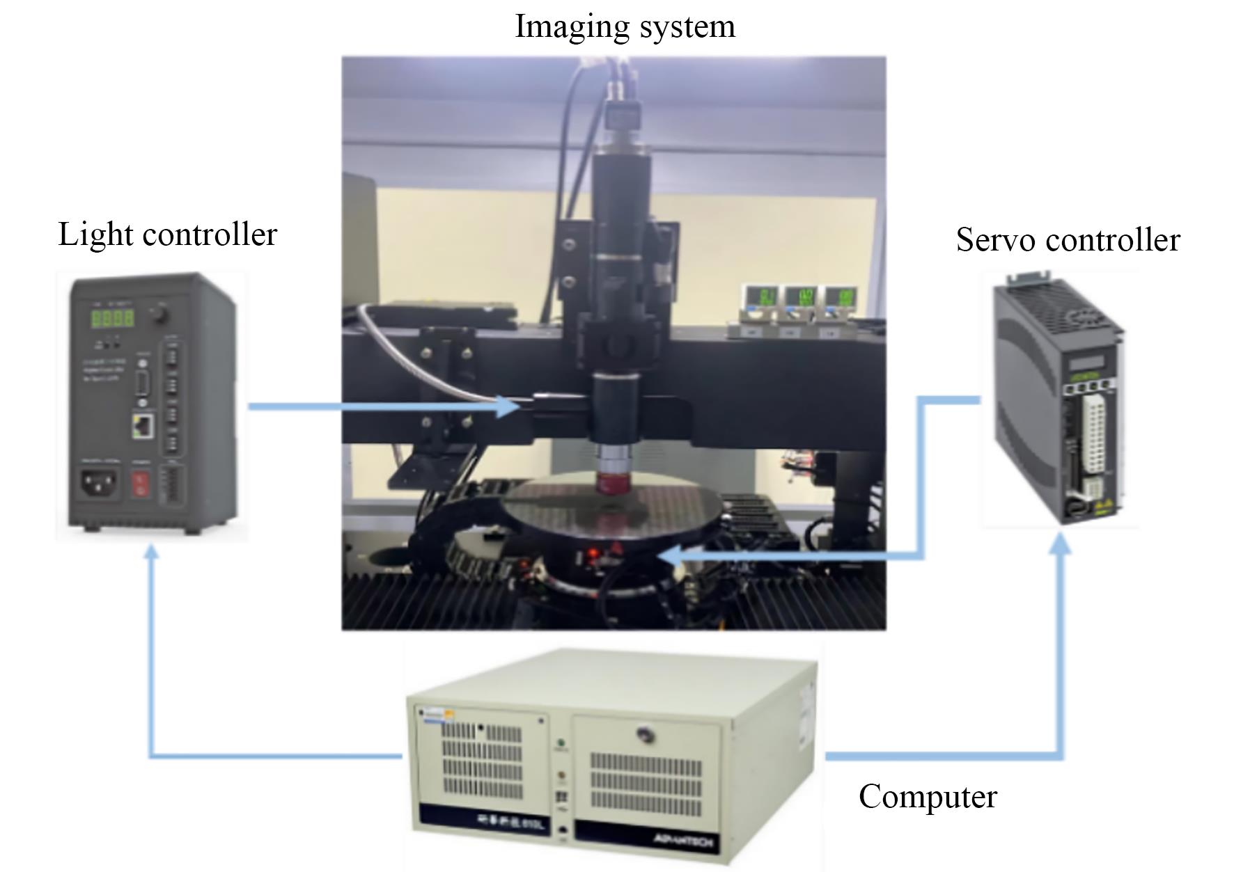
    Fig. 1. Composition of wafer motion imaging system
    Process of wafer motion imaging exposure control
    Fig. 2. Process of wafer motion imaging exposure control
    Image of typical die
    Fig. 3. Image of typical die
    Image segmentation using OTSU algorithm
    Fig. 4. Image segmentation using OTSU algorithm
    Image segmentation using blocked OTSU algorithm
    Fig. 5. Image segmentation using blocked OTSU algorithm
    Trend of classes variance with different block quantities
    Fig. 6. Trend of classes variance with different block quantities
    High and low frequency components of die images under different brightness
    Fig. 7. High and low frequency components of die images under different brightness
    Comparison of normalized evaluation values before and after Gaussian pyramid down sampling
    Fig. 8. Comparison of normalized evaluation values before and after Gaussian pyramid down sampling
    Relationship between dynamic weight and grayscale
    Fig. 9. Relationship between dynamic weight and grayscale
    Process of search algorithm
    Fig. 10. Process of search algorithm
    Pseudocode for step size selection program
    Fig. 11. Pseudocode for step size selection program
    Different evaluation curves for three types of dies
    Fig. 12. Different evaluation curves for three types of dies
    Comparison of exposure effects of different methods in different regions
    Fig. 13. Comparison of exposure effects of different methods in different regions
    ImageS1S2S2/S1
    Circuit/lead type die1.686 92.649 91.571
    Chip substrate type die1.650 12.494 21.512
    Circuit type die1.719 52.637 71.534
    Average1.685 52.593 91.539
    Table 1. Sensitivity coefficients in different regions
    MethodCircuit/lead type dieChip substrate type dieCircuit type die
    IEAVISMDIIVConsuming time/msIEAVISMDIIVConsuming time/msIEAVISMDIIVConsuming time/ms
    GH33.0123 604613 2735155.532804503 2874366.4391 979510 20244
    WDGE33.0123 604613 2735662.2521 784510 6605067.4252 226508 30152
    DCT33.0123 604613 2735261.4371 762503 0314768.2192 256516 72948
    WDFT33.5523 652620 5731962.2521 784510 6601768.2192 256516 72917
    Table 2. Best exposure image indicators obtained by different evaluation methods
    MethodCircuit/lead type dieChip substrate type dieCircuit type die
    Max search timesBest image evaluation valueIs it optimalConsuming time/sMax search timesBest image evaluation valueIs it optimalConsuming time/sMax search timesBest image evaluation valueIs it optimalConsuming time/s
    HCS27122.194Yes11746165.512Yes19631191.649Yes133
    FBS11122.194Yes4711164.95No4711191.649Yes47
    GDS7122.194Yes307164.418No307191.295No30
    CF71122.194Yes30656164.95No24166191.649Yes284
    DTS10122.194Yes4317165.512Yes7313191.649Yes56
    Table 3. Indicators for different search methods
    Ruoyu WANG, Fuyang YAN, Tundong LIU. Rapid and uniform exposure control for wafer motion imaging system[J]. Optics and Precision Engineering, 2024, 32(19): 2933
    Download Citation