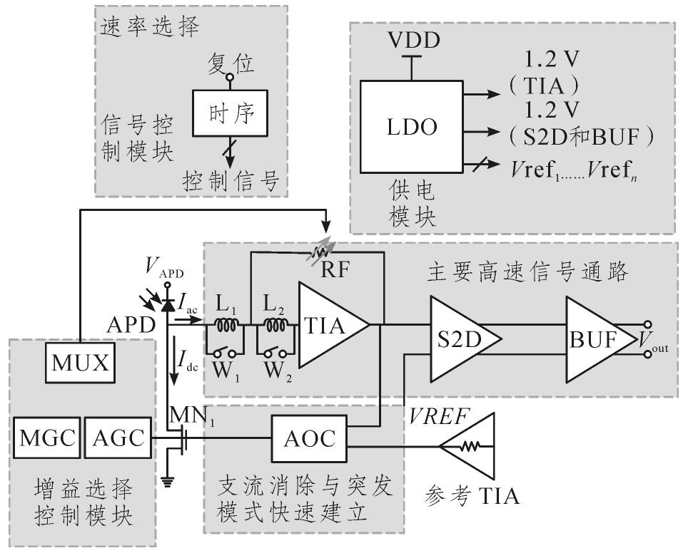
With the rapid growth in demand for high-speed Passive Optical Networks (PONs), low-cost, low-noise Burst Mode Transimpedance Amplifiers (BM-TIAs) have become a key limiting factor. In this paper, a fast-settling, low-noise BM-TIA for 10 Gigabit Symmetrical Passive Optical Network (XGS-PON) is designed based on a low-cost 40 nm Complementary Metal Oxide Semiconductor (CMOS) process, which is compatible with three signal rates: 12.5, 10.0 and 2.5 Gbit/s.
To overcome the bandwidth and noise limitations of the CMOS process, the TIA achieves the required low noise through multi-stage amplification, an input inductor balancing network, and an increased power supply voltage. The gain adjustment is achieved by a combination of feedforward amplification and feedback resistance, enabling three gain levels and rate variations. To address burst-mode signals, fast direct current cancellation loop Automatic Offset Cancellation (AOC) is used to accurately eliminate the Direct Current (DC) input from the Avalanche Photodiode (APD). The charge-sharing techniques are employed to speed up the establishment of the offset cancellation loop and suppress the baseline drift by converting the AOC loop time constant.
The chip is designed and manufactured using a 40 nm CMOS process, with a die size of 945 μm×945 μm. The chip is tested with a commercial 10 Gbit/s APD in a Transistor Outline Can (TO-CAN) package. The test results show that the sensitivity of the chip at 12.5, 10.0 and 2.5 Gbit/s is -29.7,-33.0 and -37.6 dBm, respectively. The saturated input photocurrent can reach 2.5 mA at different data rates, and the chip achieves a large input dynamic range of 24.7, 28.2 and 32.8 dB for the three data rates. The static power consumption of the chip is 82.5 mW, and the AOC settling time in burst-mode is less than 23 ns across the entire input optical power range.
This chip, applied in XGS-PON, not only provides reference for the design of low-cost and low-noise BM-TIAs based on CMOS process but also has guiding significance for chip design in higher-speed PON scenarios.


 AI Video Guide
  AI Picture Guide
 AI One Sentence


