
Yong-Liang Chen, Ya-Wen Tang, Pei-Run Chen, Li Zhang, Qi Liu, Ying Zhao, Qian Huang, Xiao-Dan Zhang. Progress in perovskite solar cells based on different buffer layer materials [J]. Acta Physica Sinica, 2020, 69(13): 138401-1
- Acta Physica Sinica
- Vol. 69, Issue 13, 138401-1 (2020)
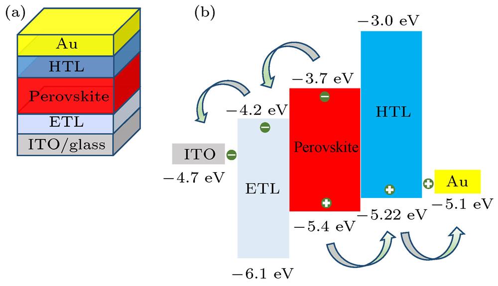
Fig. 1. Structure and energy band diagram of perovskite solar cell: (a) Structure; (b) Energy band diagram.
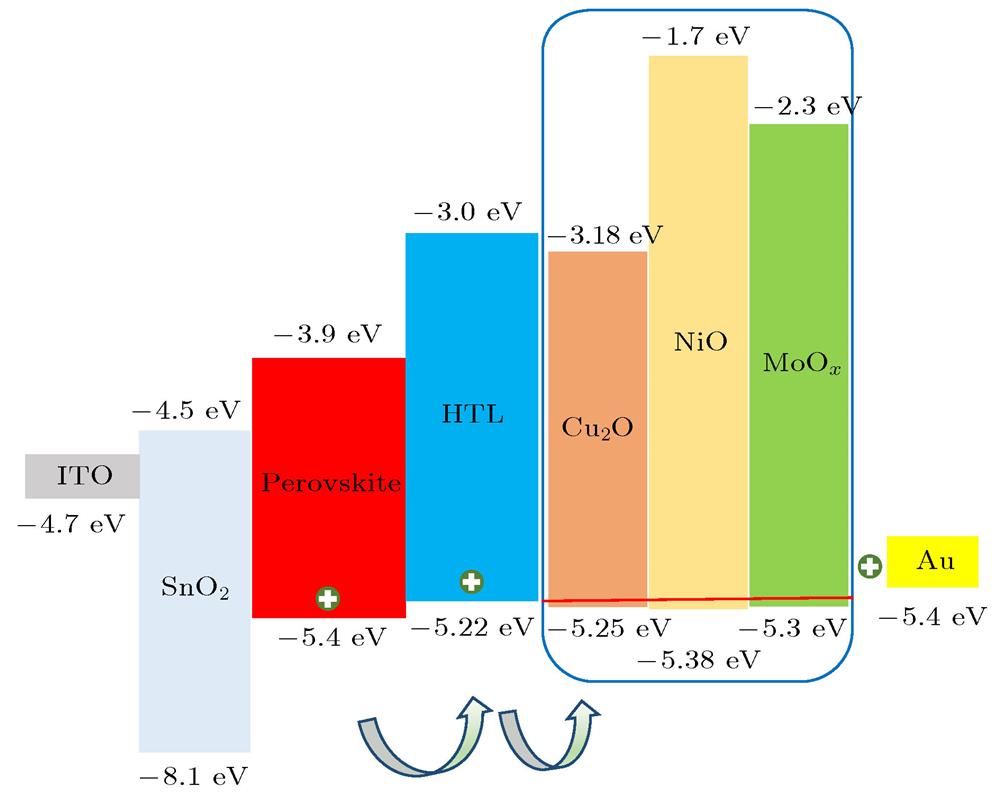
Fig. 2. Energy level diagram of the buffer layer between the hole transport layer and the anode.
Fig. 3. PCE distribution of 50 individual PSCs with and without 25 mg·ml–1 NiO buffer layer[14].
Fig. 4. Energy level diagram of the buffer layer between the electron transport layer and the cathode.
Fig. 5. I-V diagram of perovskite solar cell with different TPBi buffer layer thickness and different structure cell EQE diagram[26]: (a) I-V diagram; (b) EQE diagram.
Fig. 6. AFM diagram of Perovskite/PCBM and Perovskite/PCBM/Zr(Ac)4 films and XPS spectra showing the different amount of I, N and Pb elements on the films surface; the J-V characteristics of the optimized device perovskite solar cell with and without Zr(Ac)4 buffer layer[30]: (a) Perovskite/PCBM; (b) Perovskite/PCBM/Zr(Ac)4; (c) XPS spectra; (d) J-V diagram.
Fig. 7. The AFM images and the steady state PL spectra of ITO/PEI/SnO2/perovskite and ITO/SnO2/perovskite, and the IPCE spectra of the champion devices with and without PEI buffer layer[20]: (a) ITO/SnO2/perovskite; (b) ITO/PEI/SnO2/perovskite; (c) PL spectra; (d) IPCE spectra.
Fig. 8. Energy level diagram of the buffer layer between the hole transport layer and the absorption layer.
Fig. 9. The J-V characteristics of the optimized device and important parameter table of perovskite solar cell with GO buffer layer[33].
Fig. 10. The luminescence spectra of structure of 1: Glass/Perovskite, 2: Glass/CuPc/Perovskite, 3: Glass/CuPc/Al2O3/Perovskite and 4: Glass/CuPc/GO/Perovskite[18]
Fig. 11. Energy level diagram of the buffer layer between the electron transport layer and the absorption layer.
Fig. 12. After heating 168 hours of two different thicknesses of PCBM buffer at 85 ℃, obtained a normalized V oc, J sc, FF and PCE based on CH3NH3PbI3 absorber layer perovskite solar cells[41].
Fig. 13. XRD patterns (a) and PL spectra (b) of perovskite films on Glass/ITO/ZnO/TiO2 (x cycles) substrates with various x values[17].
Fig. 14. Steady-state photoluminescence spectra and photoluminescence decay of perovskite films with and without C60-SAM[45]: (a) PL spectra; (b) TRPL spectra.


Set citation alerts for the article
Please enter your email address

© Copyright 2018-2021 | Chinese Laser Press. All Rights Reserved 沪ICP备15018463号-20