• Laser & Optoelectronics Progress
  • Vol. 59, Issue 23, 2312004 (2022)
Yinjie Xin1,2, Quanyong Li1,2,*, Wei Sun2, Qishu Wang1,2, and Wenbo Wang1,2
Author Affiliations
  • 1Key Laboratory of Photoelectric Measurement and Optical Information Transmission Technology of Ministry of Education, School of Optoelectronic Engineering, Changchun University of Science and Technology, Changchun 130022, Jilin, China
  • 2School of Optoelectronic Engineering, Changchun University of Science and Technology, Changchun 130022, Jilin, China
  • show less
    DOI: 10.3788/LOP202259.2312004 Cite this Article Set citation alerts
    Yinjie Xin, Quanyong Li, Wei Sun, Qishu Wang, Wenbo Wang. Simulation and Error Analysis of Involute Reflector Optical Delay Line[J]. Laser & Optoelectronics Progress, 2022, 59(23): 2312004 Copy Citation Text show less
    Diagram of optical delay line of involute mirror
    Fig. 1. Diagram of optical delay line of involute mirror
    Effect of involute parameters on delay time and rotation angle
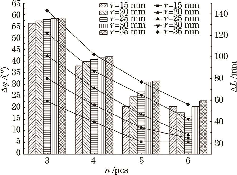
    Fig. 2. Effect of involute parameters on delay time and rotation angle
    Model diagram of rotating mirror parts. (a) Rotating axis; (b) fixing plate of rotating mirror; (c) rotating mirror; (d) rotating mirror array
    Fig. 3. Model diagram of rotating mirror parts. (a) Rotating axis; (b) fixing plate of rotating mirror; (c) rotating mirror; (d) rotating mirror array
    Optical delay line device. (a) Bearing; (b) involute reflector; (c) fixing structure; (d) bearing fixation ring; (e) optical delay line model diagram; (f) optical delay line exploded diagram
    Fig. 4. Optical delay line device. (a) Bearing; (b) involute reflector; (c) fixing structure; (d) bearing fixation ring; (e) optical delay line model diagram; (f) optical delay line exploded diagram
    Ray tracing diagram of optical delay line
    Fig. 5. Ray tracing diagram of optical delay line
    Ray tracing of optical delay line at different Δφ. (a) 0°; (b) 10°; (c) 25°; (d) 35°
    Fig. 6. Ray tracing of optical delay line at different Δφ. (a) 0°; (b) 10°; (c) 25°; (d) 35°
    Schematic diagram of eccentricity error. (a) y-axis eccentricity error; (b) x-axis eccentricity error
    Fig. 7. Schematic diagram of eccentricity error. (a) y-axis eccentricity error; (b) x-axis eccentricity error
    Plane mirror limit position with x-axis eccentricity error
    Fig. 8. Plane mirror limit position with x-axis eccentricity error
    Spot illuminance diagram of 1 mm eccentricity error. (a) y-axis 10°; (b) y-axis 25°; (c) y-axis 35°; (d) x-axis 10°; (e) x-axis 25°; (f) x-axis 35°
    Fig. 9. Spot illuminance diagram of 1 mm eccentricity error. (a) y-axis 10°; (b) y-axis 25°; (c) y-axis 35°; (d) x-axis 10°; (e) x-axis 25°; (f) x-axis 35°
    Schematic diagram of plane mirror reflection angle error
    Fig. 10. Schematic diagram of plane mirror reflection angle error
    Effect of laser divergence
    Fig. 11. Effect of laser divergence
    Ray tracing corresponding to different incident light divergence angles. (a) 0°; (b) 0.5°; (c) 1°
    Fig. 12. Ray tracing corresponding to different incident light divergence angles. (a) 0°; (b) 0.5°; (c) 1°
    Different working angle Δφ /(°)Center position of spot(xy)/(mm,mm)Spot diameter /mm
    00.00,0.002.0
    10-0.10,-0.052.5
    25-0.10,0.102.7
    35-0.10,0.052.8
    Table 1. Variation of output beam spot at different Δφ
    Yinjie Xin, Quanyong Li, Wei Sun, Qishu Wang, Wenbo Wang. Simulation and Error Analysis of Involute Reflector Optical Delay Line[J]. Laser & Optoelectronics Progress, 2022, 59(23): 2312004
    Download Citation