• Laser & Optoelectronics Progress
  • Vol. 60, Issue 15, 1514003 (2023)
Weinian Yan1,2,3, Qiuhua Wang1,3, Hengjie Zhou1,3, Pingping Qiu1,3..., Lingjuan Zhao1,2,3 and Qiang Kan1,2,3,*|Show fewer author(s)
Author Affiliations
  • 1Key Laboratory of Semiconductor Materials Science, Institute of Semiconductors, Chinese Academy of Sciences, Beijing 100083, China
  • 2College of Materials Science and Optoelectronics Engineering, University of Chinese Academy of Sciences, Beijing 100049, China
  • 3Beijing Key Laboratory of Low Dimensional Semiconductor Materials and Devices, Beijing 100083, China
  • show less
    DOI: 10.3788/LOP221703 Cite this Article Set citation alerts
    Weinian Yan, Qiuhua Wang, Hengjie Zhou, Pingping Qiu, Lingjuan Zhao, Qiang Kan. Oxide-Confined 940 nm Vertical Cavity Surface Emitting Lasers[J]. Laser & Optoelectronics Progress, 2023, 60(15): 1514003 Copy Citation Text show less
    Simulation results. (a) Material gain spectra of different barrier materials corresponding to the active region at a carrier concentration of 5×1018 cm-3 at 300 K using InGaAs as a quantum well; (b) simulated material gain spectra of the active region of InGaAs/AlGaAs at a carrier concentration of 5×1018 cm-3 at temperatures from 300 K to 400 K
    Fig. 1. Simulation results. (a) Material gain spectra of different barrier materials corresponding to the active region at a carrier concentration of 5×1018 cm-3 at 300 K using InGaAs as a quantum well; (b) simulated material gain spectra of the active region of InGaAs/AlGaAs at a carrier concentration of 5×1018 cm-3 at temperatures from 300 K to 400 K
    Simulation results. (a) Round-trip phase at different temperatures; (b) relationship between peak gain wavelength and resonant wavelength and active region temperature at different temperatures
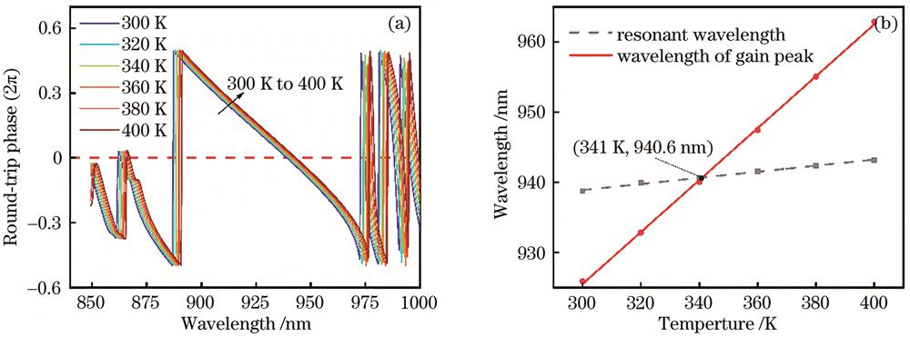
    Fig. 2. Simulation results. (a) Round-trip phase at different temperatures; (b) relationship between peak gain wavelength and resonant wavelength and active region temperature at different temperatures
    Structure diagram of top-emitting 940 nm VCSEL
    Fig. 3. Structure diagram of top-emitting 940 nm VCSEL
    Fabrication process flow chart of top-emitting 940 nm VCSEL
    Fig. 4. Fabrication process flow chart of top-emitting 940 nm VCSEL
    SEM images of top-emitting 940 nm VCSEL. (a) Device surface view; (b) device cross-sectional view;(c)infrared microscopy images of VCSELs with different oxide apertures
    Fig. 5. SEM images of top-emitting 940 nm VCSEL. (a) Device surface view; (b) device cross-sectional view;(c)infrared microscopy images of VCSELs with different oxide apertures
    940 nm VCSEL with oxide-defined apertures of 2-7 μm at room temperature. (a) P-I-V test curves; (b) PCE test curves
    Fig. 6. 940 nm VCSEL with oxide-defined apertures of 2-7 μm at room temperature. (a) P-I-V test curves; (b) PCE test curves
    Spectra of 940 nm VCSELs with different oxide-defined apertures driven by 3 mA continuous current at room temperature
    Fig. 7. Spectra of 940 nm VCSELs with different oxide-defined apertures driven by 3 mA continuous current at room temperature
    940 nm VCSELs with an oxide-defined aperture of 2 μm. (a) Spectra at different injection currents; (b) center wavelength and SMSR at different drive currents
    Fig. 8. 940 nm VCSELs with an oxide-defined aperture of 2 μm. (a) Spectra at different injection currents; (b) center wavelength and SMSR at different drive currents
    Far-field divergence angle test curves under different drive currents of 940 nm VCSEL with an oxide-defined aperture of 2 μm
    Fig. 9. Far-field divergence angle test curves under different drive currents of 940 nm VCSEL with an oxide-defined aperture of 2 μm
    940 nm VCSEL with an oxide-defined aperture of 2 μm. (a) Spectral test plots at 2 mA continuous drive current for temperatures from 10 °C to 80 ℃; (b) spectral test plots at 5 mA continuous drive current for heat sink temperatures from 10 ℃ to 80 ℃; (c) excitation center wavelength and SMSR of the device at different heat sink temperatures under 2 mA and 5 mA continuous drive currents; (d) P-I output curves of heat sink temperature from 10 ℃ to 80 ℃
    Fig. 10. 940 nm VCSEL with an oxide-defined aperture of 2 μm. (a) Spectral test plots at 2 mA continuous drive current for temperatures from 10 °C to 80 ℃; (b) spectral test plots at 5 mA continuous drive current for heat sink temperatures from 10 ℃ to 80 ℃; (c) excitation center wavelength and SMSR of the device at different heat sink temperatures under 2 mA and 5 mA continuous drive currents; (d) P-I output curves of heat sink temperature from 10 ℃ to 80 ℃
    Aperture /μmThreshold current /mAThreshold current density /(kA·cm-2Differential resistance /ΩSlope efficiency /(W·A-1Maximum output power /(mW@mA)Peak value PCE
    20.191.512870.752.67@5.0036.3%@1.02 mA
    30.381.341480.866.33@9.2039.9%@2.02 mA
    40.501.001090.938.64@12.1440.1%@3.10 mA
    50.640.82910.929.92@13.9439.8%@3.34 mA
    60.800.71820.9011.47@16.8437.1%@4.66 mA
    71.150.75660.8612.24@19.3033.5%@5.95 mA
    Table 1. Photoelectric output characteristics of VCSELs with different oxide-defined apertures at room temperature
    Temperature /℃Threshold current /mASlope efficiency /(W·A-1Maximum output power /mWDrive current /mA
    100.190.853.115.11
    200.190.782.764.94
    300.220.742.574.82
    400.250.722.354.50
    500.280.692.154.26
    600.320.671.964.16
    700.350.651.793.95
    800.420.621.593.76
    Table 2. Photoelectric output characteristics of 940 nm VCSEL with an oxide-defined aperture of 2 μm under the temperature ranging from 10 ℃ to 80 ℃
    Weinian Yan, Qiuhua Wang, Hengjie Zhou, Pingping Qiu, Lingjuan Zhao, Qiang Kan. Oxide-Confined 940 nm Vertical Cavity Surface Emitting Lasers[J]. Laser & Optoelectronics Progress, 2023, 60(15): 1514003
    Download Citation