
Chang-Fa Deng, Shao-An Yan, Dong Wang, Jin-Feng Peng, Xue-Jun Zheng. Optically modulated electromechanical coupling properties of single GaN nanobelt based on conductive atomic force microscopy [J]. Acta Physica Sinica, 2019, 68(23): 237304-1
- Acta Physica Sinica
- Vol. 68, Issue 23, 237304-1 (2019)

Fig. 1. Schematic diagram of C-AFM measurement setup.基于C-AFM的测试装置示意图
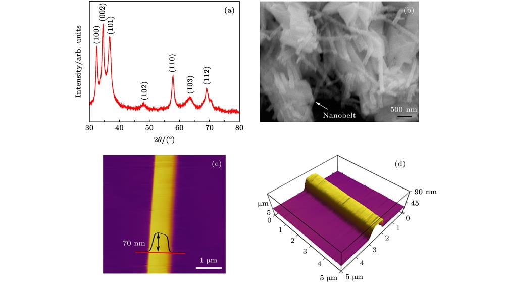
Fig. 2. (a) XRD scans and (b) SEM image of the as-prepared GaN nanobelt powder; (c) 2-D and (d) 3-D AFM morphology image of a single GaN nanobelt.(a) GaN纳米带粉末XRD图谱; (b) GaN纳米带粉末SEM图像; (c)单根GaN纳米带AFM二维形貌图及(d)三维形貌图
Fig. 3. (a)−(c) 2-D current topography of a single GaN nanobelt under dark condition with the loading forces of 30 nN, 50 nN and 70 nN, respectively; (d)−(f) 2-D current topography of a single GaN nanobelt under light condition with the loading forces of 30 nN, 50 nN and 70 nN, respectively. The insert shows the current value at the cross section of 2-D current topography.(a)−(c)暗场下单根GaN纳米带的二维电流形貌图, 加载力分别为30, 50, 70 nN; (e)−(f)光场下单根GaN纳米带的二维电流形貌图, 加载力分别为30, 50, 70 nN; 插图为电流形貌图截面处的电流值
Fig. 4. Single point I -V curves of a single GaN nanobelt: (a), (b) I -V curve and its logarithmic coordinate with different loading forces under dark condition; (c), (d) I -V curve and its logarithmic coordinate with different loading forces under light condition.
GaN纳米带单点I -V 曲线 (a), (b)暗场不同加载力下的I -V 曲线及对数坐标形式; (c), (d)光场不同加载力下的I -V 曲线及对数坐标形式
Fig. 5. I -t curves of a single GaN nanobelt under different loading forces in light and dark conditions: (a) 30 nN; (b) 40 nN.
明暗场不同加载力下单根GaN纳米带的I -t 曲线 (a) 30 nN; (b) 40 nN
Fig. 6. (a) Schematic diagram of equivalent circuit of the single GaN nanobelt based device; (b) schematic diagram of energy band structure with optically modulated electromechanical coupling.(a)单根GaN纳米带器件等效电路示意图; (b)光力电耦合能带结构示意图


Set citation alerts for the article
Please enter your email address

© Copyright 2018-2021 | Chinese Laser Press. All Rights Reserved 沪ICP备15018463号-20