• Photonics Research
  • Vol. 2, Issue 3, A19 (2014)
Takanori Shimizu1,2,*, Nobuaki Hatori1,2, Makoto Okano1,3, Masashige Ishizaka1,2..., Yutaka Urino1,2, Tsuyoshi Yamamoto1,2, Masahiko Mori1,3, Takahiro Nakamura1,2 and and Yashuhiko Arakawa4|Show fewer author(s)
Author Affiliations
  • 1Institute for Photonics-Electronics Convergence System Technology (PECST), Japan
  • 2Photonics Electronics Technology Research Association (PETRA), West 7SCR, 16-1 Onogawa, Tsukuba, Ibaraki 305-8569, Japan
  • 3National Institute of Advanced Industrial Science and Technology (AIST), West 7SCR, 16-1 Onogawa, Tsukuba, Ibaraki 305-8569, Japan
  • 4Institute of Industrial Science, The University of Tokyo, 4-6-1 Komaba, Meguro, Tokyo 153-8505, Japan
  • show less
    DOI: 10.1364/PRJ.2.000A19 Cite this Article Set citation alerts
    Takanori Shimizu, Nobuaki Hatori, Makoto Okano, Masashige Ishizaka, Yutaka Urino, Tsuyoshi Yamamoto, Masahiko Mori, Takahiro Nakamura, and Yashuhiko Arakawa, "Multichannel and high-density hybrid integrated light source with a laser diode array on a silicon optical waveguide platform for interchip optical interconnection," Photonics Res. 2, A19 (2014) Copy Citation Text show less
    Schematic of integrated light source in photonics-electronics convergence system.
    Fig. 1. Schematic of integrated light source in photonics-electronics convergence system.
    Hybrid integration structure with an LD array on a silicon waveguide platform.
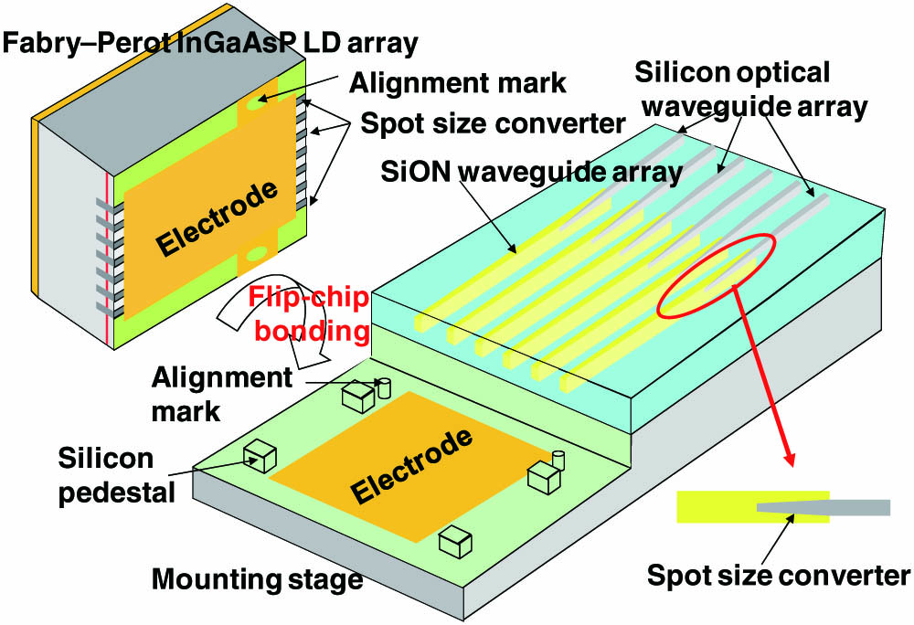
    Fig. 2. Hybrid integration structure with an LD array on a silicon waveguide platform.
    Photograph of 13-channel LD array. Cavity length is 400 μm, and array pitch is 30 μm.
    Fig. 3. Photograph of 13-channel LD array. Cavity length is 400 μm, and array pitch is 30 μm.
    Scanning electron microscope image of waveguide facet made by dry etching.
    Fig. 4. Scanning electron microscope image of waveguide facet made by dry etching.
    (a) Schematic of LD mounting structure and (b) LD mounting image focused on alignment marks by transmission infrared light.
    Fig. 5. (a) Schematic of LD mounting structure and (b) LD mounting image focused on alignment marks by transmission infrared light.
    (a) Schematic and (b) photograph of 13-channel hybrid integrated light source.
    Fig. 6. (a) Schematic and (b) photograph of 13-channel hybrid integrated light source.
    Dependence of light output of 13-channel LD array on operating current at room temperature without cooling.
    Fig. 7. Dependence of light output of 13-channel LD array on operating current at room temperature without cooling.
    Optical coupling tolerance between LD and SiON waveguide along horizontal and vertical directions.
    Fig. 8. Optical coupling tolerance between LD and SiON waveguide along horizontal and vertical directions.
    Relative light intensity of 13-channel LD array and waveguide output ports on integrated light source.
    Fig. 9. Relative light intensity of 13-channel LD array and waveguide output ports on integrated light source.
    (a) Schematic and (b) photograph of integrated light source with 52 output ports made possible by introducing waveguide splitter.
    Fig. 10. (a) Schematic and (b) photograph of integrated light source with 52 output ports made possible by introducing waveguide splitter.
    Schematic showing multichip bonding technology. (a) Mounting structure and (b) illustration of diffusion of Au on surface of electrodes into AuSn bump at soldering.
    Fig. 11. Schematic showing multichip bonding technology. (a) Mounting structure and (b) illustration of diffusion of Au on surface of electrodes into AuSn bump at soldering.
    (a) Schematic and (b) photograph of integrated light source with 104 output ports with two LD array chips.
    Fig. 12. (a) Schematic and (b) photograph of integrated light source with 104 output ports with two LD array chips.
    Near-field pattern of outputs in integrated light source with 104 output ports.
    Fig. 13. Near-field pattern of outputs in integrated light source with 104 output ports.
    Histogram of relative intensity of output ports. (a) 1st–52nd channel port and (b) 53rd–104th channel port.
    Fig. 14. Histogram of relative intensity of output ports. (a) 1st–52nd channel port and (b) 53rd–104th channel port.
    RequirementsTarget
    High densityNarrow pitch<1/10 conventional laser array
    Small footprint/ch<0.01mm2/ch
    MultichannelMultichannel/chip13 ch
    Multi-chip10–20 chip
    splitter1×4, 1×8
    High powerHigh laser power>10mW/ch
    Low coupling loss2–3 dB
    Table 1. Requirements of Integrated Light Source for 10Tbit/s Optical Interconnects
    Takanori Shimizu, Nobuaki Hatori, Makoto Okano, Masashige Ishizaka, Yutaka Urino, Tsuyoshi Yamamoto, Masahiko Mori, Takahiro Nakamura, and Yashuhiko Arakawa, "Multichannel and high-density hybrid integrated light source with a laser diode array on a silicon optical waveguide platform for interchip optical interconnection," Photonics Res. 2, A19 (2014)
    Download Citation