
Chuanhua DU, Binghuang DUAN, Cen XIONG, Chao ZENG. Transient radiation response of SOI transistors and SOI devices[J]. NUCLEAR TECHNIQUES, 2024, 47(4): 040402
- NUCLEAR TECHNIQUES
- Vol. 47, Issue 4, 040402 (2024)
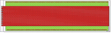
Fig. 1. Layout of the tested device

Fig. 2. Photocurrent IDS vs. drain-source voltage VDS irradiated with different laser energies for the three types of transistors
Fig. 3. Waveform of measured photocurrent IDS of drain-source under different laser energies for two types of transistors(a) 0.35 μm SOI NMOS, (b) 0.35 μm Si NMOS
Fig. 4. MCU test circiut
Fig. 5. Block diagram of gamma dose rate test method for MCU circuit
Fig. 6. Transient dose rate radiation response of the square wave signal of an MCU circuit (dose rate: 4.2×10¹¹ rad(Si)·s-1)
Fig. 7. Transient source current of an MCU circuit(dose rate: 4.2×10¹¹ rad(Si)·s-1)
Fig. 8. Transient dose rate response of the 3.3 V MCU voltage (dose rate: 4.2×10¹¹ rad(Si)·s-1)
Fig. 9. Transient dose rate response of the 1.2 V MCU voltage (dose rate: 4.2×10¹¹ rad(Si)·s-1)
Fig. 10. Transient dose rate response of an oscillator voltage (dose rate: 4.2×10¹¹ rad(Si)·s-1)
Fig. 11. Test results of logic states of a trigger flip-flop chain after gamma irradiation
Fig. 12. Schematic diagram of sensitive charge collect volume for bulk Si (a) and SOI MOS (b)
|
Table 1. Information on laser-tested devices


Set citation alerts for the article
Please enter your email address

© Copyright 2018-2021 | Chinese Laser Press. All Rights Reserved 沪ICP备15018463号-20