
Jie TAN, Shibin LIU, Jiezhang LUO, Yinghao CHEN, Yongqian Du. Research progress of light addressable potentiometric sensor with optimized structure[J]. Optics and Precision Engineering, 2022, 30(16): 1924
- Optics and Precision Engineering
- Vol. 30, Issue 16, 1924 (2022)
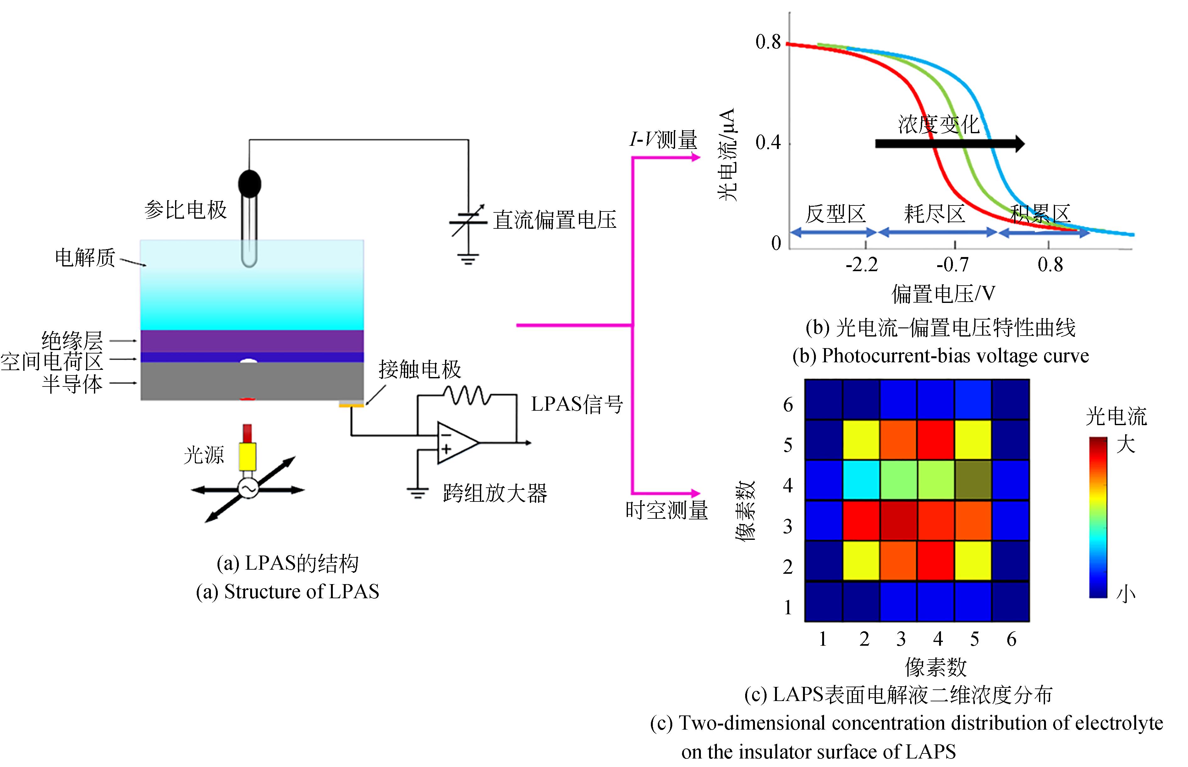
Fig. 1. Structure and working principle of LAPS
![Setup picture of ultra-high speed chemical imaging system based on analog micromirror[29]](/richHtml/gxjmgc/2022/30/16/1924/img_2.jpg)
Fig. 2. Setup picture of ultra-high speed chemical imaging system based on analog micromirror[29]
Fig. 3. Optimization of LAPS with porous insulator[62]
Fig. 4. Comparison of LAPS with anodic oxidized insulator and LAPS with thermal oxidized insulator[64]
Fig. 5. Normalized photocurrent line scan curves across SU-8 edge using SOS substrate with undecylenic acid grafted onto silicon layers with different thickness[65-66]
Fig. 6. Performance test of LAPS fabricated by ICP-RIE[82]
Fig. 7. Chemical image and spatial resolution of LAPS using InGaN/GaN as a semiconductor layer[89]
Fig. 8. Comparison of chemical imaging of LAPS with honeycomb meshed working electrodes and LAPS with the flat working electrodes[96]
Fig. 9. Performance test of ES-LAPS using ITO as the semiconductor layer[97]
Fig. 10. Time-lapse photocurrent images of B50 cells exposed to 0.01% TX-100 in S-HEPES buffer[101]
|
Table 1. Important research results of LAPS in insulator optimization
|
Table 2. Important research results of optimization of LAPS using silicon as the semiconductor layer
|
Table 3. Important research results of optimization of LAPS using non-silicon as the semiconductor layer
|
Table 4. Important research results of LAPS in electrodes optimization
|
Table 5. Important research results of ES-LAPS


Set citation alerts for the article
Please enter your email address

© Copyright 2018-2021 | Chinese Laser Press. All Rights Reserved 沪ICP备15018463号-20