
Mane-Si Laure Lee, Julie Cholet, Anne Delboulbé, Raphaël Guillemet, Brigitte Loiseaux, Patrick Garabédian, Thomas Flügel-Paul, Tino Benkenstein, Susann Sadlowski, Nicolas Tetaz, Roman Windpassinger, Ana Baselga Mateo. Wide band UV/Vis/NIR blazed-binary reflective gratings for spectro-imagers: two lithographic technologies investigation[J]. Journal of the European Optical Society-Rapid Publications, 2023, 19(1): 2023004
Journals >Journal of the European Optical Society-Rapid Publications >Volume 19 >Issue 1 >Page 2023004 > Article
- Journal of the European Optical Society-Rapid Publications
- Vol. 19, Issue 1, 2023004 (2023)
Abstract
Keywords
1 Introduction
Next generation of spectro-imagers for future Earth observation missions requests ultra-wide band operation, very large field of view but small volume. However, the performance of these future instruments is limited by the performance of the diffraction grating, since high diffraction efficiency and reduced polarization sensitivity over wide spectral range are required, while introducing a limited wavefront error (WFE). In this paper, we report on gratings with period of 30 μm and operating at an angle of incidence of 0.5°, matching the specific requirements of a Dyson spectrometer [
| Spectral band | 340–1040 nm |
|---|---|
| Diffraction efficiency in the −1st diffraction order | λ = 340 nm: >0.5 |
| λ = 440 nm: >0.4 | |
| λ = 800 nm: >0.35 | |
| λ = 1040 nm: >0.35 | |
| Polarization sensitivity | <10% (goal < 1%) |
| Spectral ghosts intensities | <1e−4 (with respect to useful diffracted order) |
| Wavefront error | WFE < 100 nm RMS |
Table 1. Grating requirements related to UV/Vis/NIR spectro-imager.
Classical continuous reflective saw-tooth profile blazed-gratings offer peak efficiencies up to ~90% (mainly limited by the reflectivity of the metallic material) but it decreases significantly when approaching the band edges in the ultraviolet (UV) and near-infrared (NIR) regions. To overcome this limited spectral efficiency, several approaches have been proposed in the literature. The first approach consists of combining several materials to achromatize the efficiency. Originally proposed for transmission gratings [
A third type of approach is based on blazed-binary gratings composed of subwavelength structures [
Here, we evaluate the optical performance of blazed-binary gratings manufactured by two lithography techniques: e-beam and nanoimprint lithography (NIL) and compare their performance with next generation spectro-imager requirements, which are summarized in
E-beam lithography has shown its ability for the manufacturing of transmission type blazed-binary gratings for the Gaia Space Mission [
NIL is a less mature technology, as compared to e-beam lithography. However, the progress of the NIL equipment and process enables now the patterning of very small resolution features. As a replication technology, NIL enables fast and cost-effective manufacturing process fitted for low/medium-volume for earth observation missions.
2 Subwavelength gratings fabrication
The design of blazed-binary subwavelength gratings is based on artificial distributed-index media engineering [
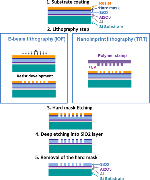
The gratings realization uses the same process steps, except for the lithography step. The process flow is depicted in
![]()
Figure 1.Process flow for the realization of the blazed-binary gratings.
We use a lithography step to define the patterns into a resist layer, followed by dry etching processes to i) transfer the patterns into the metal mask and ii) to transfer the patterns into the underlying SiO2 material and get high aspect ratio structures.
Regarding the lithography step, two techniques were investigated: 1) e-beam lithography at Fraunhofer Institute for Applied Optics and Precision Engineering (IOF), which is the most common technique to tackle such small size patterns and 2) NIL at Thales Research & Technology (TRT). The NIL is a replication technology which consists of fabricating a transparent polymer stamp (polydimethylsiloxane PDMS) and applying the stamp onto a photosensitive resist layer cured under UV light. The polymer stamp which is illustrated in
![]()
Figure 2.Silicon master (4″) (a) and manufactured PDMS mold (b) fixed on a thin glass plate (c) used for the NIL grating manufacturing.
The advantage of NIL enables the same high resolution as e-beam lithography, with reduced process time (typically few minutes per wafer vs. few hours). Pictures of two gratings are given in
![]()
Figure 3.Manufactured gratings on 4″ wafer by e-beam lithography (a) and on 3″ wafer by NIL (b). (c) SEM top view of few subwavelength structures of the NIL grating.
3 Optical measurements
The ~80 mm diameter blazed-binary subwavelength gratings were characterized optically at IOF premises.
The efficiency measurements were performed using a tunable light source. The gratings are illuminated by a monochromatic light beam (diameter: ~3 mm) with adaptable wavelength (FWHM < 5 nm). Measurements are carried out under transverse electric (TE) and transverse magnetic (TM) polarization. The diffracted light is detected using an integrating sphere which is mounted on a goniometer setup.
![]()
Figure 4.Spatial mapping of the diffraction efficiency in −1st order of the prototype flat grating for three different wavelengths, i.e. 376 nm (a), 600 nm (b) and 1000 nm (c).
![]()
Figure 5.Measured −1st order diffraction efficiency of blazed-binary subwavelength gratings.
From
First, both e-beam and NIL give similar efficiency behavior which is in average 10–20% above the requirement (red line).
Secondly, the proposed design (green line) and subwavelength grating technology (black and blue line) are tolerant to height deviation of 50 nm (blue line) and efficiency remains compatible with requirements.
![]()
Figure 6.Polarization sensitivity of the blazed-binary subwavelength gratings.
It results that the polarization sensitivity is smaller than 2% for both gratings over the whole spectral band, which confirms experimentally subwavelength optics polarization property.
E-beam technology is well-known for its ability to achieve low level grating ghosts [
![]()
Figure 7.Angular scanning of the efficiency in the diffractive plane at 633 nm for the NIL blazed-binary grating.
The diffracted orders are separated by Δθ ≈ 1.3° and the −1st order is located at θ = −6.3°. It results that no additional peak is visible, meaning that no grating ghosts are measured. Note that this result is not surprising as the NIL technology uses a master based on e-beam lithography. However, it shows that the NIL technology does not introduce additional ghosts.
The wavefront error (WFE) introduced by the fabrication process is evaluated by measuring the reflected WFE of the gratings, using a plane-wave Zygo Verifire AT 12″ interferometer at a wavelength of 633 nm.
The wavefront deformation introduced by the fabrication process is evaluated as follows: 1) the retro-reflected wavefront of the grating is measured for collimated illumination obeying Littrow condition. A first measurement is performed in +1st diffraction order and a second measurement is independently performed in −1st diffraction order. 2) Both wavefront maps are then subtracted. This allows removing the influence of the grating substrate’s deformation. The result only covers the inaccuracy introduced by the respective patterning process (see
![]()
Figure 8.Reflected wavefront introduced by the grating fabrication process (excluding substrate deformation) for e-beam grating (a) and for NIL grating (b).
For both technologies, the WFE is smaller than 20 nm RMS, which is 5 times smaller than the 100 nm RMS space application requirement.
To our knowledge, although NIL technology is less mature than e-beam lithography, it is the first time that such excellent WFE over 3″ size component is measured.
4 Outlook towards curved substrates
The next generation of hyperspectral imagers will need to operate over very wide spectral bands and large fields of view, while being very compact and lightweight. For this purpose, architectures using a spherical grating such as Offner or Dyson type are of interest. So it is important to investigate the routes towards manufacturing blazed-binary gratings on spherical substrate.
Several approaches have been proposed for echelette-type spherical gratings fabrication. One approach is based on “multi-zone” e-beam writing for the fabrication of a convex (radius of 88 mm) echelette grating operating in 400 nm–1 μm [
To go towards spherical substrates for blazed-binary subwavelength gratings, two approaches, depicted in
![]()
Figure 9.Two identified routes for blazed-binary subwavelength grating fabrication on spherical substrate. (a) Thinning and bonding of a flat grating on a spherical substrate. (b) NIL on spherical substrate.
In this paper, we focus on the second approach. The first step to validate is the lithography step, i.e. the use of NIL on spherical substrate. We present hereafter preliminary replication tests to validate the use of NIL on spherical substrate, by controlling the geometry of the replicated pattern and its uniformity over the spherical substrate. For this purpose, we first applied the PDMS flexible stamp into a resist layer coated on a 3″ 540 mm-radius concave silica substrate, with a home-made equipment. The resist is then exposed to UV illumination and the stamp pattern is transferred into the resist layer, step 2 in
![]()
Figure 10.Preliminary NIL replication tests on concave (R = 540 mm) substrate. (a) Picture of the 3″ resist patterned area. (b) Scanning electron microscope photograph of the grating pattern (in resist layer).
The challenge for nanoimprint technology on spherical substrate is to ensure a homogeneous pressure over the substrate to achieve the suitable uniformity of the pattern dimension uniformity. To check the pattern uniformity, we have measured the pillars and holes widths from SEM photographs taken within five zones of the substrate.
![]()
Figure 11.Location of the measurements zones, within the substrate.
To quantify the uniformity, we have measured the holes and pillars width dispersion on five zones with respect to the average width over the five zones. In total, we have proceeded to the measurements for 44 different geometries included into one period of the grating: 31 pillars having widths varying between 180 nm to 330 nm and 13 holes having widths varying between 160 nm and 330 nm are measured. For each geometry, the measured width is the average of six measurements.
![]()
Figure 12.Measured width dispersion of the replicated patterns on different zones of the 3″ concave substrate. Horizontal axis corresponds to the number of the patterns. Each series of points corresponds to the zones of
From the graph of
The optimization of the process to ensure a good uniformity is still under investigation and constitutes the main manufacturing challenge for the next generation of gratings.
5 Conclusion and perspectives
We have studied and characterized wide spectral band and large area 3″ blazed-binary subwavelength reflective gratings based on a same design that have been manufactured by two technologies: e-beam lithography and NIL. They are composed of high aspect ratio (~5), high density and one level subwavelength binary structures.
Optical measurements show that the subwavelength blazed-binary gratings approach and manufacturing processes based on either e-beam or nanoimprint technologies are very promising for space application. They enable superior performance, in term of spectral band (efficiency margin of 10–20% in average), polarization sensitivity (<2%), very low ghost level (not detectable), and WFE level (<20 nm RMS) with respect to requirements for observation spectro-imagers operating in UV/Vis/NIR.
As next step will be to address the grating manufacturing on spherical substrate to enable more performant spectro-imager architectures, we also investigated the challenge of nanoimprint on spherical substrate. Results of nanoimprint replication done on a 540 mm-radius concave substrate show that NIL technology enable uniformity better than ±20 nm over the 3″ surface. Such result obtained for large radius of curvature (~500 mm) are very promising as the main challenge is related to uniform application of the flexible stamp with a homogeneous pressure over the spherical substrate. This is the first time to our knowledge that such experimental demonstration and measurements, based on NIL replication of high density pattern, composed of mixed pillars and holes with different size ranging from 160 nm to 330 nm, arranged on a 500 nm grid, and on a 3″ concave substrate, are reported.
References
[1] N. Tetaz, C. Ruilier, M. Taccola, T. Viard, M.-S.L. Lee Bouhours, B. Loiseaux, G. Lehoucq. Advanced large FOV UV/VIS/NIR/SWIR spectrometers for future earth observation instruments.
[2] S.M. Ebstein. Achromatic diffractive optical elements.
[3] B.H. Kleemann, M. Seesselberg, J. Ruoff. Design concepts for broadband high-efficiency DOEs.
[4] O. Sandfuchs, M. Kraus, R. Brunner. Structured metal double-blazed dispersion grating for broadband spectral efficiency achromatization.
[5] P. Mouroulis, S.W. Wilson, P.D. Maker, R.E. Muller. Convex grating types for concentric imaging spectrometers.
[6] B. Van Gorp, P. Mouroulis, D.W. Wilson, R.O. Green. Design of the compact wide swath imaging spectrometer (CWIS).
[7] C. Sauvan, P. Lalanne, M.-S.L. Lee. Broadband blazing with artificial dielectrics.
[8] C. Ribot, M.-S.L. Lee, S. Collin, S. Bansropun, P. Plouhinec, D. Thenot, S. Cassette, B. Loiseaux, P. Lalanne. Broadband and efficient diffraction.
[9] F. Burmeister, T. Flügel-Paul, U.D. Zeitner, M.-S.L. Lee-Bouhours, G. Lehoucq, J. Cholet, B. Loiseaux, N. Tetaz, R. Windpassinger, M. Taccola. Binary blazed reflection grating for UV/VIS/NIR/SWIR spectral range.
[10] M. Erdmann, E.-B. Kley, U. Zeitner. Development of a large blazed transmission grating by effective binary index modulation for the GAIA radial velocity spectrometer.
[11] W. Stork, N. Streibl, H. Haidner, P. Kipfer. Artificial distributed-index media fabricated by zero-order gratings.
[12] M. Heusinger, M. Banasch, T. Flügel-Paul, U.D. Zeitner. Investigation and optimization of Rowland ghosts in high efficiency spectrometer gratings fabricated by e-beam lithography.
[13] D.W. Wilson, P.D. Maker, R.E. Muller, P.Z. Mouroulis, J. Backlund. Recent advances in blazed grating fabrication by electron-beam lithography.
[14] D.W. Wilson, R.E. Muller, P.M. Echternach, J.P. Backlund. Electron-beam lithography for micro and nano-optical applications.
[15] F. Zamkotsian, I. Zhurminsky, P. Lanzoni, N. Tchoubaklian, F. Lütolf, M. Schnieper, C. Schneider, S. Fricke, M. Fouchier, M. Zerrad, C. Amra, V. Costes, J. Loesel. Blazed gratings on convex substrates for high throughput spectrographs for Earth and Universe observation.
[16] T. Flügel-Paul, C. Rothhardt, T. Benkenstein, K. Grabowski, S. Risse, R. Eberhardt, B. Guldimann, U.D. Zeitner. All-dielectric Prism-Grating-Prism component realized by direct hydrophilic bonding technology for optical applications in space.
[17] P. Birckigt, K. Grabowski, G. Leibeling, T. Flügel-Paul, M. Heusinger, H. Ouslimani, S. Risse. Effects of static load and residual stress on fused silica direct bonding interface properties.


Set citation alerts for the article
Please enter your email address

© Copyright 2018-2021 | Chinese Laser Press. All Rights Reserved 沪ICP备15018463号-20