
Cheng Zhang, Yin Xu, Yue Dong, Bo Zhang, Yi Ni. Lithium Niobate Waveguide Mode Converter Based on V-Shaped Silicon[J]. Laser & Optoelectronics Progress, 2024, 61(5): 0523001
- Laser & Optoelectronics Progress
- Vol. 61, Issue 5, 0523001 (2024)
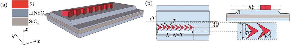
Fig. 1. The proposed LNOI-based waveguide mode converter using V-shaped silicon. (a) Schematic; (b) top and side view
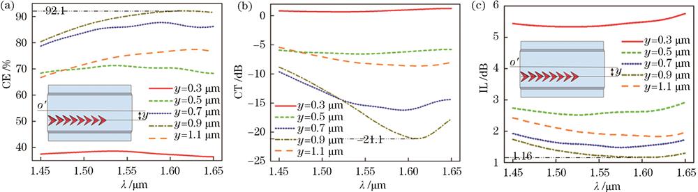
Fig. 2. Device performance dependent on the deviation distance y of the array. (a) Mode conversion efficiency; (b) mode crosstalk; (c) insertion loss
Fig. 3. Device performance dependent on the period number N and period T of the V-shaped silicon.(a)N=18;(b)N=14;(c)N=16;(d)N=20;(e)N=22;(f)N=24
Fig. 4. Width w and sag length d of the V-shaped silicon affecting on the device performance.(a)d=0.8 μm;(b)d=0.4 μm;(c)d=0.6 μm;(d)d=1 μm;(e)d=1.2 μm;(f)d=1 μm,w=400 nm
Fig. 5. Device performance dependent on the thickness h of the silicon array.(a)h=100 nm;(b)h =150 nm;(c)h=200 nm;(d)h=250 nm;(e)h=300 nm;(f)h=250 nm,T=500 nm
Fig. 6. The improvement effect of period T on device performance. (a) Mode conversion efficiency; (b) bandwidth analysis
Fig. 7. Electric field evolution of the proposed TFLN waveguide based TE0-to-TE1 mode converter
Fig. 8. Device performance dependent on key dimensions. (a) Sag length d;(b) width w; (c) thickness h
Fig. 9. Electric field evolution of the proposed TFLN waveguide based TE0-to-TE2 mode converter
|
Table 1. Structural parameters of proposed TFLN waveguide based TE0-to-TE1 mode converter
|
Table 2. Structural parameters of proposed TFLN waveguide based TE0-to-TE2 mode converter


Set citation alerts for the article
Please enter your email address

© Copyright 2018-2021 | Chinese Laser Press. All Rights Reserved 沪ICP备15018463号-20