• Chinese Optics Letters
  • Vol. 22, Issue 9, 091301 (2024)
Jiaqi Wang1,*, Yingqi Xu1, Zhijian Mao1, Guoxian Wu1..., Rongxiang Guo2,3, Xu Li1, Yu Du1, Youfu Geng1, Xuejin Li1, Hon Ki Tsang4 and Zhenzhou Cheng2,3,5,6,**|Show fewer author(s)
Author Affiliations
  • 1College of Physics and Optoelectronic Engineering, Shenzhen University, Shenzhen 518060, China
  • 2School of Precision Instrument and Optoelectronics Engineering, Tianjin University, Tianjin 300072, China
  • 3Key Laboratory of Optoelectronics Information Technology, Ministry of Education, Tianjin 300072, China
  • 4Department of Electronic Engineering, The Chinese University of Hong Kong, Hong Kong, China
  • 5Georgia Tech-Shenzhen Institute, Tianjin University, Shenzhen 518055, China
  • 6School of Physics and Electronic Engineering, Xinjiang Normal University, Urumqi 830054, China
  • show less
    DOI: 10.3788/COL202422.091301 Cite this Article Set citation alerts
    Jiaqi Wang, Yingqi Xu, Zhijian Mao, Guoxian Wu, Rongxiang Guo, Xu Li, Yu Du, Youfu Geng, Xuejin Li, Hon Ki Tsang, Zhenzhou Cheng, "Optical bistability in a silicon nitride microring integrated with 2D PtSe2 [Invited]," Chin. Opt. Lett. 22, 091301 (2024) Copy Citation Text show less
    Schematic of the PtSe2-on-silicon nitride MRR. (a) Three-dimensional view of the device; (b) top view of the device; (c) cross-sectional view of the waveguide.
    Fig. 1. Schematic of the PtSe2-on-silicon nitride MRR. (a) Three-dimensional view of the device; (b) top view of the device; (c) cross-sectional view of the waveguide.
    Characterization of the five-layer PtSe2 on the surface of the silicon nitride chip. (a) The AFM characterization of the PtSe2 film; (b) the Raman spectrum of the PtSe2 film measured using a Raman spectrometer with a pump wavelength of 785 nm; (c) the measurement result of the XPS full spectrum; the Gaussian fitting curves of (d) Se 3d peak and (e) Pt 4f peak in (c).
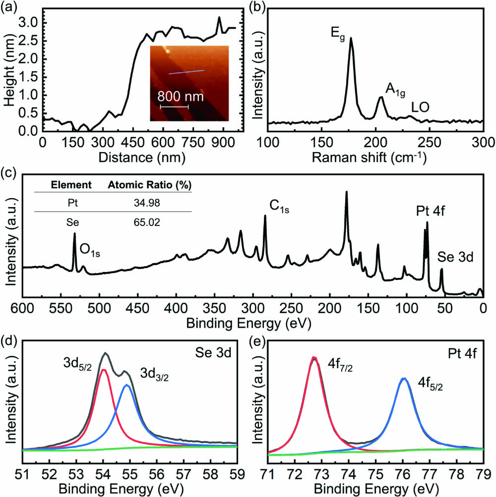
    Fig. 2. Characterization of the five-layer PtSe2 on the surface of the silicon nitride chip. (a) The AFM characterization of the PtSe2 film; (b) the Raman spectrum of the PtSe2 film measured using a Raman spectrometer with a pump wavelength of 785 nm; (c) the measurement result of the XPS full spectrum; the Gaussian fitting curves of (d) Se 3d peak and (e) Pt 4f peak in (c).
    Characterization of the PtSe2-on-silicon nitride MRRs. (a) and (d) the SEM images of two MRRs with the PtSe2 film coverage, with estimated lengths of the material covered of 125 and 471 µm. (b) and (c) The transmission spectra of the MRR in (a) before and after the PtSe2 film transfer; (e) and (f) the transmission spectra of the MRR in (d) before and after the PtSe2 film transfer.
    Fig. 3. Characterization of the PtSe2-on-silicon nitride MRRs. (a) and (d) the SEM images of two MRRs with the PtSe2 film coverage, with estimated lengths of the material covered of 125 and 471 µm. (b) and (c) The transmission spectra of the MRR in (a) before and after the PtSe2 film transfer; (e) and (f) the transmission spectra of the MRR in (d) before and after the PtSe2 film transfer.
    Optical nonlinearity measurement and simulation results. (a) Schematic of the experimental setup; (b) measured transmission spectra at different input power levels; (c) resonant wavelengths at different input powers; (d) simulated transmission spectra at different input powers using the time-domain CMT method; (e) simulated resonant wavelengths at different input powers; (f)–(h) hysteresis loop simulations for the input wavelengths of 1541.55, 1541.56, and 1541.57 nm; arrows in (f)–(h) indicate the directions of the input power variations.
    Fig. 4. Optical nonlinearity measurement and simulation results. (a) Schematic of the experimental setup; (b) measured transmission spectra at different input power levels; (c) resonant wavelengths at different input powers; (d) simulated transmission spectra at different input powers using the time-domain CMT method; (e) simulated resonant wavelengths at different input powers; (f)–(h) hysteresis loop simulations for the input wavelengths of 1541.55, 1541.56, and 1541.57 nm; arrows in (f)–(h) indicate the directions of the input power variations.
    Electromagnetic thermal simulation results of the waveguide cross section. Temperature distributions of (a) the PtSe2-on-silicon nitride waveguide cross section and (b) the bare waveguide cross section.
    Fig. 5. Electromagnetic thermal simulation results of the waveguide cross section. Temperature distributions of (a) the PtSe2-on-silicon nitride waveguide cross section and (b) the bare waveguide cross section.
    ParameterValueSource
    Q05800[Measurement]
    Qext40324[Measurement, CMT[27,28]]
    Qinst6774[Measurement, CMT[27,28]]
    τlinear (s)1.6 × 10⁻⁹[Measurement, CMT[27,28]]
    R (K/mW)105[Measurement, CMT[27,28]]
    n01.9965[Reference[29]]
    n2 (m2/W)2.6 × 10−19[Reference[30]]
    ng2.05[FDTD simulation]
    V (m3)8.4754 × 10⁻¹⁶[FDTD simulation]
    ∂n/∂T (1/K)2.51 × 10−5[Reference[31]]
    Table 1. Parameters and Sources Used in CMT Simulation
    Jiaqi Wang, Yingqi Xu, Zhijian Mao, Guoxian Wu, Rongxiang Guo, Xu Li, Yu Du, Youfu Geng, Xuejin Li, Hon Ki Tsang, Zhenzhou Cheng, "Optical bistability in a silicon nitride microring integrated with 2D PtSe2 [Invited]," Chin. Opt. Lett. 22, 091301 (2024)
    Download Citation