【AIGC One Sentence Reading】:We developed a III-V-on-silicon-nitride mode-locked laser, tunable across 1530-1580 nm, using heterogeneous integration. Precise spectrum control and a 23-nm-wide emission with a 10 dB bandwidth at 3 GHz repetition rate were achieved.
【AIGC Short Abstract】:We have developed a III-V-on-silicon-nitride mode-locked laser using heterogeneous integration. By optimizing the lasing wavelength and exploring the electrical driving parameters, we achieved precise control of the optical spectrum across a wide wavelength range. Additionally, through Monte Carlo-based optimization, we obtained a laser emitting a broad spectrum while maintaining a defined bandwidth for a high pulse repetition rate.
Note: This section is automatically generated by AI . The website and platform operators shall not be liable for any commercial or legal consequences arising from your use of AI generated content on this website. Please be aware of this.
Abstract
We demonstrate a III-V-on-silicon-nitride mode-locked laser through the heterogeneous integration of a semiconductor optical amplifier on a passive silicon-nitride cavity using the technique of micro-transfer printing. In the initial phase of our study, we focus on optimizing the lasing wavelength to be centered at 1550 nm. This optimization is achieved by conducting experiments with 27 mode-locked lasers, each incorporating optical amplifiers featuring distinct multiple-quantum-well photoluminescence values. Subsequently we present a comprehensive study investigating the behavior of the mode-locking regime when the electrical driving parameters are varied. Specifically, we explore the impact of the gain voltage and saturable absorber current on the locking stability of a tunable mode-locked laser. By manipulating these parameters, we demonstrate the precise control of the optical spectrum across a wide range of wavelengths spanning from 1530 to 1580 nm. Furthermore, we implement an optimization approach based on a Monte Carlo analysis aimed at enhancing the mode overlap within the gain region. This adjustment enables the achievement of a laser emitting a 23-nm-wide spectrum while maintaining a defined 10 dB bandwidth for a pulse repetition rate of 3 GHz.
Author Presentation Playback
1. INTRODUCTION
Mode-locked lasers find extensive applications across various fields, such as distance measurements [1,2], spectroscopy [3], holography [4], telecommunications [5,6], or bio-sensing [7]. While efficient fiber [8] or solid-state bulk lasers [9,10] are commonly used in these systems, there is growing interest in on-chip solutions due to their potential for cost reduction and compact footprint. Recent technological advancements [11] have led to successful demonstrations of electrically pumped on-chip mode-locked lasers in both monolithic III-V [12] and heterogeneous III-V-on-silicon platforms [13–15]. These developments open up exciting possibilities, enabling miniaturization and enhanced functionality for a wide range of applications. However, the performance of these lasers in terms of pulse energy and noise is limited by the relatively high waveguide losses as well as by two-photon absorption and the associated free-carrier absorption. Fortunately, silicon nitride exhibits low waveguide losses and negligible two-photon absorption at telecom wavelengths [16], making it a promising platform for the demonstration of heterogeneous III-V-on-silicon-nitride electrically pumped mode-locked lasers with improved performance. However, state-of-the-art III-V-on-silicon-nitride mode-locked lasers have suffered from relatively narrow optical spectra. For instance, previous studies have reported mode-locked optical spectra centered at 1582 nm and 1610 nm, with 10 dB bandwidths of 3.27 nm and 4 nm, respectively [17,18]. This limited spectral bandwidth can restrict the potential applications. Ongoing research and development efforts are focused on addressing this limitation and improving the performance of on-chip mode-locked lasers to achieve wider and tunable optical spectra. Another approach is to generate a soliton microcomb, as shown in Refs. [19,20]. In that case a heterogeneous laser is used to pump a SiN high- ring resonator. The characteristics of the combs are interesting, and such combs have already been used as a microwave generator by beating two-comb lines, but the reported microring soliton combs provide a low density of comb lines (FSR in the range of 30–100 GHz) limiting the possibilities for some dual-comb applications, such as spectroscopy. Furthermore, the demonstration has been done using the technology of the direct wafer-bonding approach for heterogeneous integration. This technology is today pretty mature but is still asking efforts in the postprocessing of the active material and is not optimizing the use of the costly material. For future systems, wafer bonding also limits the possibility in terms of integrating several different active materials on the same CMOS platform.
In this study, we present a III-V-on-silicon-nitride mode-locked laser by heterogeneously integrating a III-V semiconductor optical amplifier onto a passive silicon-nitride cavity using the versatile technique of micro-transfer printing. A review of micro-transfer-printing technology, including a comparison with other heterogeneous integration techniques, such as wafer-bonding and flip-chip integration, can be found in Ref. [21].
Our primary focus is to optimize the lasing wavelength, aiming for a centered emission at 1550 nm. To achieve this, we perform experiments with 27 mode-locked lasers, incorporating optical amplifiers with different multiple-quantum-well photoluminescence values of 1480, 1495, and 1520 nm. Through systematic testing, we identify the optimal photoluminescence wavelength that results in the desired centered emission wavelength at 1550 nm. Additionally, we conduct a comprehensive study to investigate the behavior of the mode-locking regime when the electrical driving parameters are varied. Specifically, we explore the effects of the gain voltage and saturable absorber current on the stability of the mode-locked laser. By adjusting these parameters, we demonstrate the control of the optical spectrum over a wide range of wavelengths from 1530 to 1580 nm. Furthermore, we implement an optimization approach to improve the mode confinement within the gain region. This adjustment allows us to achieve a laser with a centered emission wavelength of 1550 nm while keeping a 23-nm-wide 10-dB bandwidth optical spectrum and operating at a pulse repetition rate of 3 GHz. These parameters collectively enable the generation of more than 1000 optical lines.
Sign up for Photonics Research TOC. Get the latest issue of Photonics Research delivered right to you!Sign up now
2. DESIGN OF THE PASSIVE EXTENDED LASER CAVITY AND INTEGRATION OF THE GAIN
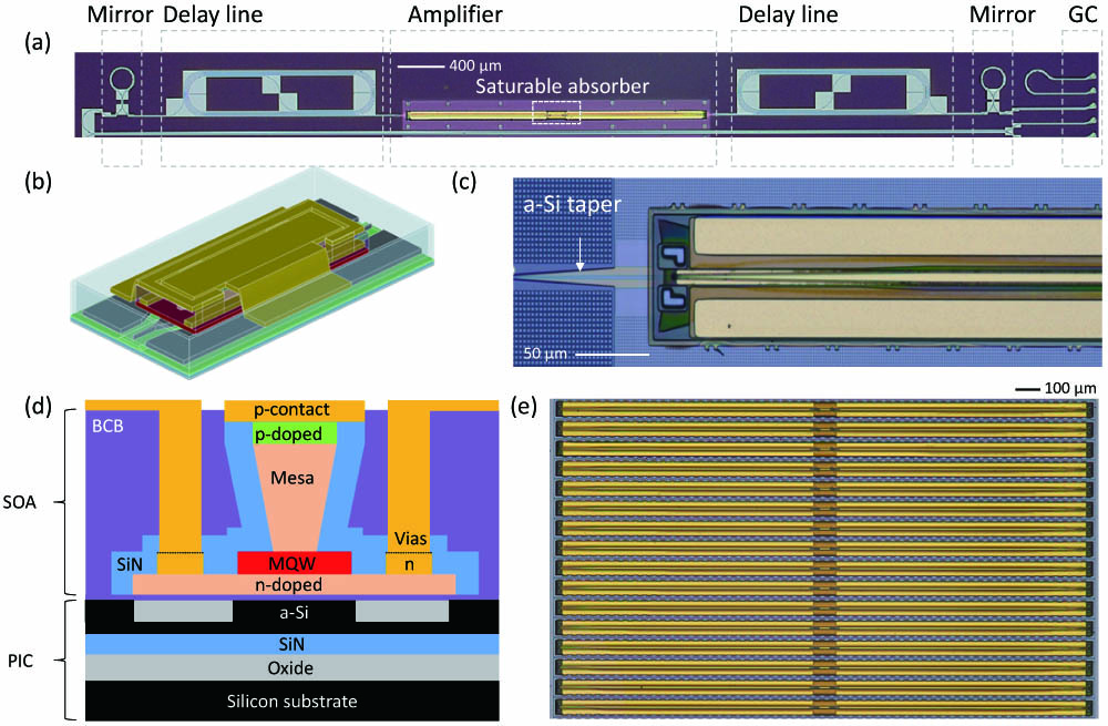
The mode-locked lasers employed in this study utilize a combination of a passive cavity and an active gain region, which incorporates a saturable absorber section. The integration of the active device onto the passive circuit is achieved through the technique of micro-transfer printing. This process involves the picking and placement of suspended source coupons onto a host target, allowing for heterogeneous integration at the technological back-end level. This technique is suitable for the integration of thin films [22–24] and preprocessed devices [18–21]. For more in-depth information on the micro-transfer-printing technique, including its methodology and implementation, we refer interested readers to Ref. [21]. Here we describe the composition of both the passive photonic circuit and the active device used in our mode-locked laser. Figure 1(a) provides a visual representation of the integrated laser cavity, showcasing the successful integration of the gain section using the micro-transfer-printing technique.
Figure 1.(a) View of the mode-locked laser circuit, composed of two Sagnac loop mirrors, two delay lines, a semiconductor optical amplifier including a saturable absorber, and a grating coupler (GC). (b) Schematic view of the semiconductor optical amplifier. (c) Optical microscope picture of the semiconductor optical amplifier micro-transfer printed on the passive laser cavity. (d) Composition of passive photonic integrated circuit (PIC) and active semiconductor optical amplifier (SOA) of the laser. (e) Optical microscope pictures of the suspended semiconductor optical amplifiers. This sample is used as the source sample in the micro-transfer-printing process.
The passive circuit is designed as an extended laser cavity, which is implemented on 200 mm silicon wafers with 2200 nm of oxide, a 400-nm-thick LPCVD silicon-nitride layer, and a thin film of amorphous silicon (a-Si, described later). The light propagating within the cavity is guided through a 1100-nm-wide silicon-nitride box waveguide. Based on measurements on 850-nm-wide box waveguides, the waveguide loss in the cavity is expected to be better than 0.25 dB/cm. The laser cavity includes two Sagnac loop mirrors with nominal reflections of 30% and 100%. Two low-footprint spiral waveguides are used, providing a total cavity length of 4.3 cm SiN and 0.3 cm a-Si/III-V corresponding to a repetition rate of 3 GHz. In a mode-locked laser, the repetition rate is directly related to the cavity length. In order to have a dense comb of lines, we are taking advantage of the low loss SiN extended cavity to build a laser over 5-cm of cavity length, making it possible to reach a low repetition rate. This is an important parameter to consider, for example, when targeting spectroscopy. Tapered waveguides enable coupling between the SiN and a-Si layer with a measured transmission of . Coupling to fiber is enabled by fully etched, low-back-reflection grating couplers with a measured efficiency of at 1550 nm wavelength. In the design, we incorporate two evanescent adiabatic coupling sections to facilitate efficient transfer of light between the silicon-nitride spiral waveguides and the III-V gain waveguide. The first coupling section enables the coupling of light from the silicon-nitride waveguide to an amorphous silicon waveguide, while the second coupling section facilitates the coupling of the optical signal from the amorphous silicon waveguide to the gain medium. For further details on the two-step evanescent adiabatic coupling in silicon-nitride integrated laser systems, we refer to Refs. [25,26]. A schematic view of the evanescent coupling structure is depicted in Fig. 1(b), while Fig. 1(c) shows a microscope picture of the amorphous silicon taper used to couple the optical signal from the silicon nitride to the amplifier.
The active device is a 2.5-mm-long semiconductor optical amplifier based on indium phosphide lattice matched materials [27]. It incorporates a multiple-quantum-well structure composed of InAlGaAs periodically grown layers, in between -type and -type cladding layers. The specific design of the multiple-quantum-well is tailored to achieve the desired photoluminescence wavelength. To facilitate the transfer-printing process, the epitaxial stack includes a release layer. This layer enables the suspension of the amplifier coupons, allowing for their integration through the micro-transfer-printing technique. Electrical contacts are directly deposited on the and layers of the device, enabling electrical connections. For mechanical stability and support, the semiconductor optical amplifier is encapsulated with a layer of silicon nitride. Mechanical tethers are patterned to ensure that the device remains suspended after wet etching of the release layer. The composition of the laser is illustrated in the schematic of Fig. 1(d). An optical microscope image depicting the suspended active devices after the release wet etching process is shown in Fig. 1(e). It is worth noting that the amplifier includes an electrically isolated section at its center, achieved through local dry-etching of the layers. This isolated section is 100 μm long and plays a crucial role in providing the saturable absorption effect, which is essential for achieving mode locking in the laser. While the gain section is electrically pumped through a forward bias, enabling the creation of electron-hole pairs for gain, the saturable absorber section can be biased in reverse to facilitate the desired saturable absorption effect.
3. OPTIMIZATION OF THE LASING WAVELENGTH
To effectively control the lasing characteristics of the mode-locked lasers, a preliminary investigation into the lasing wavelength is undertaken. The lasing wavelength in laser design is influenced by both the passive cavity and the gain device. Although optical propagation in the silicon-nitride waveguides is well understood, the complexities of the III-V amplifier and saturable absorber impede the prediction of the lasing wavelength in on-chip mode-locked laser diodes. However, it is feasible to precisely manipulate the photoluminescence wavelength of the multiple-quantum-well structure. A set of mode-locked lasers is subsequently manufactured, employing semiconductor optical amplifiers with distinct photoluminescence wavelengths of 1480, 1495, and 1520 nm.
The lasers are biased using a PGSGP probe, which is connected to two Keithley instruments. One is employed to apply forward bias to the gain section using a current, while the other is used to apply backward bias to the saturable absorber section through a voltage. The optical signal generated by the laser is then extracted from the cavity using a grating coupler and split using a 10/90 fiber coupler. The optical signal from the 10% branch is collected by a power meter for measurement, while the optical signal from the 90% branch is equally divided and directed into an optical spectrum analyzer and a fast photodiode operating at 40 GHz. The output of the photodiode is connected to an electrical spectrum analyzer for further analysis. Finally, the center wavelengths of 37 stable mode-locking optical spectra have been recorded (all the successful working devices are presented there), and correlated with the photoluminescence wavelength of the semiconductor optical amplifiers. The mode locking is verified by analyzing the profile of the optical-to-radio-frequency converted frequency comb. The results of the measurements are presented in Fig. 2(a). For photoluminescence wavelengths of 1480 nm, 1495 nm, and 1550 nm, the lasing wavelengths cover the range of 1530–1550 nm, 1540–1570 nm, and 1570–1610 nm, respectively. This graphic is teaching us that to achieve a lasing wavelength around 1550 nm, which is commonly used in commercially available low-cost photonic devices, the photoluminescence wavelength of the semiconductor optical amplifier should be 1495 nm. Furthermore, for some applications, for example, in spectroscopy, it remains interesting to be able to design the system for any lasing wavelength of interest fitting molecular transitions. The radio-frequency signal confirming the mode-locking, obtained after down-conversion in the fast photodiode, is depicted in Fig. 2(b). Figure 2(c) shows a zoom on the first peak at 2.987 GHz, for passive and hybrid mode-locking (when the saturable absorber is driven by an RF source at a frequency equal to the repetition rate of the laser) configurations, while the corresponding optical spectrum recorded can be observed in Fig. 2(d). The output power of the laser depends on the current provided to the SOA. When the current is increased, the output power also increases, but around 300 mA, the heating of the amplifier induces thermal effects leading to a degradation in the laser’s performance and the power starts to decrease again when increasing the current. This also affects the lasing wavelength of the laser, making it possible to tune the spectra by varying the current. Both effects are shown on Fig. 2(d).
Figure 2.(a) Measurements of the center wavelength of 37 mode-locking spectra generated by the mode-locked lasers as a function of the photoluminescence wavelength. (b) Example of an optical-to-radio-frequency converted spectrum showing the mode-locking behavior of the laser. (c) Zoom-in of the repetition frequency signal with a center frequency of 2.987 GHz (RBW is 1 kHz) for passive and hybrid mode-locking. (d) Example of a recorded optical spectrum.
In this section, we study in more detail the behavior of a mode-locked laser utilizing a semiconductor optical amplifier with a photoluminescence wavelength of 1495 nm. The radio-frequency spectra of different lasing modes are analyzed as a function of the gain driving parameters while varying the gain current and the saturable absorber voltage. The laser exhibits various modes of operation, which have been labeled as , and . These labels distinguish the different operating regimes observed. Figure 3(a) provides a summary of the modes for each combination of gain and saturable absorber parameters with a resolution of 10 mA for the gain and 0.1 V for the saturable absorber. The modes are distinguished by their profile of the associated radio-frequency spectrum. An example of the profile of each of the modes is presented in Fig. 3(b).
Figure 3.(a) Figure of merit of the mode-locking operation of the laser as a function of the gain current and the saturable absorber bias voltage. (b) Example of radio-frequency spectra for each operation mode described on figure (a) labeled , and . (c) Example of optical spectra generated by the laser under different driving parameters for mode , when the laser is mode-locking. The driving parameters for each spectrum can be extracted from (a). (d) Center wavelength of the optical spectra as a function of the applied gain current and corresponding average power coupled in the fiber.
The laser is optimized to operate at a repetition rate of 3 GHz. When the laser is mode locked, a comb of lines can be observed in the radio-frequency domain according to the following relation:
Here, represents the frequency of the lines, is the repetition rate of 3 GHz, and is an integer. The mode corresponds to laser operation without achieving the mode locking. In that case, some lines appear at random positions in the radio-frequency spectrum. For the mode the lines from Eq. (1) are observed along with an extra 30 dB less parasitic comb of lines following the Eq. (2):
The mode is the mode corresponding to the desired mode-locking of the laser. We can notice that it appears for the widest area of driving parameters in Fig. 3(a), showing the stability of the laser. Mode is similar to mode , but with a repetition rate of 6 GHz, corresponding to the second harmonic of the fundamental repetition rate of 3 GHz. Mode is a clean comb of lines following Eq. (1) with a repetition rate of 6 GHz. Here we only present a descriptive observation of the laser behavior, but, in future work, an understanding study involving statistics over a large range of laser measurements should be conducted to clarify the physical reasons behind the observed mode jumping. Figure 3(c) displays optical spectra recorded for mode of the laser. The laser can generate optical spectra with different wavelengths ranging from 1530 to 1580 nm, depending on the amplifier driving parameter settings influencing the self-heating of the device. It is worth noting that all of these spectra were recorded from the same laser using different driving parameters demonstrating the tunability of the mode-locked laser presented in this work. The relationship between the center wavelength of the generated spectra and the gain current applied to the semiconductor optical amplifier is depicted in Fig. 3(d).
5. OPTIMIZATION OF THE MODE CONFINEMENT IN THE MULTIPLE-QUANTUM-WELL
In a last study, we optimize the confinement in the multiple-quantum-well of the semiconductor optical amplifier of the hybrid amorphous-silicon-III-V optical mode. The confinement depends on the geometrical parameters of the amorphous silicon waveguide, i.e., the amorphous silicon waveguide thickness, the waveguide width, and the shallow etching depth, and on its refractive index.
The quantum-well confinement influences the properties of the laser. The parameters to consider are the following: the gain (high confinement means high gain, i.e., 2.9%);the saturable absorption (high confinement means saturable absorption, i.e., 2.9%);the saturation power (high confinement means low saturation power, i.e., 1.5%).
To have a laser with decent output power, we ideally need to have a high quantum-well confinement [following the item (i)]. This also allows us to reach the mode-locking via the saturable absorption effect [following the item (ii)]. But as a trade-off, the quantum-well confinement cannot be too strong; otherwise the saturation power is too low [following the item (iii)].
We do not currently have a model showing the influence of the parameters on the mode-locking, but our study tends to show experimentally the effect of the quantum-well confinement and allows us to find what is the best quantum-well confinement to have a stable mode-locked laser. We could think about an advanced design, where the confinement is different for the gain section and the saturable absorber section, but this is not investigated here.
Furthermore, it is very important to take into consideration the undesired variations of the parameters coming from the fabrication uncertainties.
The overlap between the optical mode and the multiple-quantum-well is then optimized via a Monte Carlo analysis. We calculate the overlap for three different geometries, based on an amorphous silicon thickness of 370 nm, 350 nm, and 330 nm, respectively. In each case, we defined a set of 60 parameter combinations that accounted for variations from the nominal values following a 3-sigma normal distribution. The relevant variations we considered were as follows: the amorphous silicon thickness , the waveguide width , the shallow etching depth , and the refractive index . Figure 4(a) presents the results of the analysis. The mode overlap with the multiple-quantum-well has median values of 1.4%, 2%, and 2.9% for an amorphous silicon layer thickness of 370 nm, 250 nm, and 330 nm, respectively. The corresponding propagation loss, coming from the absorption in the metal of the amplifier, is also computed [Fig. 4(b)] and has in all the cases a median value below 1.7 dB/cm, corresponding to less than half a decibel loss for an amplifier 2.5 mm long. A representation of the hybrid amorphous-silicon-III-V mode is depicted in Fig. 4(c) for an amorphous silicon thickness of 350 nm.
Figure 4.(a) Simulation of the multiple-quantum-well confinement for three thicknesses of amorphous silicon (370 nm, 350 nm, and 330 nm) for a set of 60 geometrical parameter variations following a deviation from a nominal value through a 3-sigma normal distribution. (b) Associated modal loss. (c) Hybrid optical mode for an amorphous silicon thickness of 350 nm, corresponding to 2% of multiple-quantum-well confinement.
Mode-locked lasers with different thicknesses of the amorphous silicon intermediate layer are measured. The optical spectra generated by the lasers, in the case of mode-locking with a repetition rate of 3 GHz, are compared together in Fig. 5. The widest optical spectrum is then obtained for an amorphous silicon thickness of 350 nm, corresponding to a mode confinement in the multiple-quantum-well of 2%. The spectrum is as wide as 23 nm for a 10 dB bandwidth, meaning that the laser exhibits more than 1000 comb lines.
Figure 5.Comparison between measured optical spectra, generated near 1550 nm, for different multiple-quantum-well optical confinement factors.
We have demonstrated a III-V-on-silicon-nitride mode-locked laser with a wide optical spectrum of 23 nm, optimized to emit around 1550 nm. Furthermore, we have demonstrated various operating regimes by modifying the gain current and saturable absorber voltage. In addition, the significance of the multiple-quantum-well confinement factor was illustrated experimentally. For later optimization, one could think about designing the laser with different confinement factors for the gain section and the saturable absorber section. In addition, it is also possible to stabilize thermal effects by incorporating thermal vias, while maintaining control over tuning through local heaters [11,15]. These developments pave the way to develop improved on-chip mode-locked laser diodes with enhanced control over the emitting wavelengths while achieving a broad comb bandwidth with more than 1000 optical comb lines. These properties are essential to build practical dual-comb devices on a photonic chip, targeting applications such as dual-comb spectroscopy [28,29] and dual-comb ranging [26], amongst others. Furthermore, exploring recent developments in the proven enhancement of the gain medium for lasers using quantum dots [30] could pave the way for the next generation of extended cavity heterogeneous mode-locked lasers.
[24] T. Vanackere, M. Billet, C. O. de Beeck. Micro-transfer printing of lithium niobate on silicon nitride. European Conference on Optical Communications (ECOC), 1-4(2020).
[29] K. V. Gasse, Z. Chen, E. Vincentini. Dual-comb spectroscopy with two on-chip III-V-on-silicon 1-GHz mode-locked lasers. Conference on Lasers and Electro-Optics, SM3A.7(2021).
 AI Video Guide
  AI Picture Guide
 AI One Sentence