
Maximilien Billet, Stijn Cuyvers, Stijn Poelman, Artur Hermans, Sandeep Seema Saseendra, Tasuku Nakamura, Shinya Okamoto, Yasuhisa Inada, Kazuya Hisada, Taku Hirasawa, Joan Ramirez, Delphine Néel, Nicolas Vaissière, Jean Decobert, Philippe Soussan, Xavier Rottenberg, Gunther Roelkens, Jon Ø. Kjellman, Bart Kuyken, "Heterogeneous tunable III-V-on-silicon-nitride mode-locked laser emitting wide optical spectra," Photonics Res. 12, A21 (2024)
- Photonics Research
- Vol. 12, Issue 3, A21 (2024)
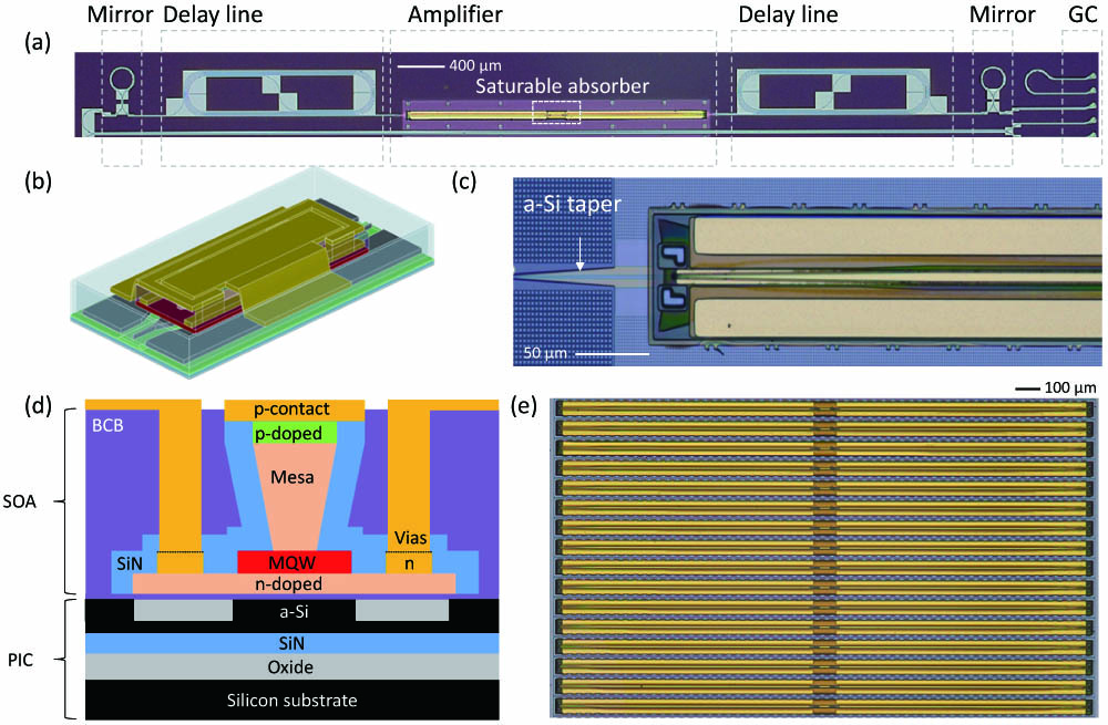
Fig. 1. (a) View of the mode-locked laser circuit, composed of two Sagnac loop mirrors, two delay lines, a semiconductor optical amplifier including a saturable absorber, and a grating coupler (GC). (b) Schematic view of the semiconductor optical amplifier. (c) Optical microscope picture of the semiconductor optical amplifier micro-transfer printed on the passive laser cavity. (d) Composition of passive photonic integrated circuit (PIC) and active semiconductor optical amplifier (SOA) of the laser. (e) Optical microscope pictures of the suspended semiconductor optical amplifiers. This sample is used as the source sample in the micro-transfer-printing process.

Fig. 2. (a) Measurements of the center wavelength of 37 mode-locking spectra generated by the mode-locked lasers as a function of the photoluminescence wavelength. (b) Example of an optical-to-radio-frequency converted spectrum showing the mode-locking behavior of the laser. (c) Zoom-in of the repetition frequency signal with a center frequency of 2.987 GHz (RBW is 1 kHz) for passive and hybrid mode-locking. (d) Example of a recorded optical spectrum.
Fig. 3. (a) Figure of merit of the mode-locking operation of the laser as a function of the gain current and the saturable absorber bias voltage. (b) Example of radio-frequency spectra for each operation mode described on figure (a) labeled M 0 , M 1 , M 2 , M 3 M 4 M 2
Fig. 4. (a) Simulation of the multiple-quantum-well confinement for three thicknesses of amorphous silicon (370 nm, 350 nm, and 330 nm) for a set of 60 geometrical parameter variations following a deviation from a nominal value through a 3-sigma normal distribution. (b) Associated modal loss. (c) Hybrid optical mode for an amorphous silicon thickness of 350 nm, corresponding to 2% of multiple-quantum-well confinement.
Fig. 5. Comparison between measured optical spectra, generated near 1550 nm, for different multiple-quantum-well optical confinement factors.


Set citation alerts for the article
Please enter your email address

© Copyright 2018-2021 | Chinese Laser Press. All Rights Reserved 沪ICP备15018463号-20