• Photonics Research
  • Vol. 12, Issue 1, 154 (2024)
Yuxin Yang1,†, Jiaxin Gao1,†, Hao Wu1, Zhanke Zhou1..., Liu Yang1, Xin Guo1,2,4,*, Pan Wang1,2 and Limin Tong1,2,3,5,*|Show fewer author(s)
Author Affiliations
  • 1Interdisciplinary Center for Quantum Information, New Cornerstone Science Laboratory, State Key Laboratory of Extreme Photonics and Instrumentation, College of Optical Science and Engineering, Zhejiang University, Hangzhou 310027, China
  • 2Jiaxing Key Laboratory of Photonic Sensing & Intelligent Imaging, Intelligent Optics & Photonics Research Center, Jiaxing Research Institute Zhejiang University, Jiaxing 314000, China
  • 3Collaborative Innovation Center of Extreme Optics, Shanxi University, Taiyuan 030006, China
  • 4e-mail: guoxin@zju.edu.cn
  • 5e-mail: phytong@zju.edu.cn
  • show less
    DOI: 10.1364/PRJ.506681 Cite this Article Set citation alerts
    Yuxin Yang, Jiaxin Gao, Hao Wu, Zhanke Zhou, Liu Yang, Xin Guo, Pan Wang, Limin Tong, "Generating a nanoscale blade-like optical field in a coupled nanofiber pair," Photonics Res. 12, 154 (2024) Copy Citation Text show less
    (a) Schematic illustration of generating a nanoscale blade-like optical field in a CNP. (b) Close-up profile of the field around the slit in (a). The inset illustrates cross-sectional distribution of the polarized charge density.
    Fig. 1. (a) Schematic illustration of generating a nanoscale blade-like optical field in a CNP. (b) Close-up profile of the field around the slit in (a). The inset illustrates cross-sectional distribution of the polarized charge density.
    Four lowest eigenmodes of the As2S3 CNP waveguide. Normalized electric field distribution and surface polarized bound charge density distribution of (a) TE0-like, (b) TM0-like, (c) TE1-like, and (d) TM1-like modes in an As2S3 CNP with D=200 nm at 640 nm wavelength, respectively. The white arrows indicate the electric field vectors of the modes. The scale bar in (a) applies to (b)–(d). (e)–(g) Diameter-dependent neff of the four lowest modes of a free-standing CNP at (e) 640 nm, (f) 1550 nm, and (g) 4.5 μm wavelength, respectively. The light-yellow-shaded areas represent the selected diameter areas in this work. The dashed black lines indicate the refractive index of the air.
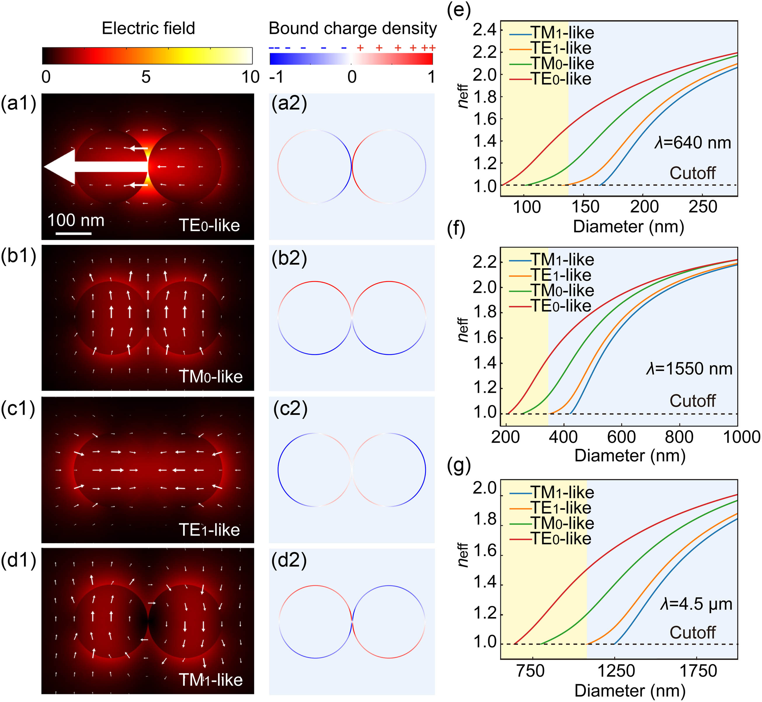
    Fig. 2. Four lowest eigenmodes of the As2S3 CNP waveguide. Normalized electric field distribution and surface polarized bound charge density distribution of (a) TE0-like, (b) TM0-like, (c) TE1-like, and (d) TM1-like modes in an As2S3 CNP with D=200  nm at 640 nm wavelength, respectively. The white arrows indicate the electric field vectors of the modes. The scale bar in (a) applies to (b)–(d). (e)–(g) Diameter-dependent neff of the four lowest modes of a free-standing CNP at (e) 640 nm, (f) 1550 nm, and (g) 4.5 μm wavelength, respectively. The light-yellow-shaded areas represent the selected diameter areas in this work. The dashed black lines indicate the refractive index of the air.
    Sub-nm-confined optical fields in the nano-slit mode of an As2S3 CNP. (a) 3D plot of the normalized cross-sectional field intensity distribution of the TE0-like nano-slit mode of an As2S3 CNP with D=300 nm and W=1 nm at 1550 nm wavelength. (b), (c) Field intensity distribution along the horizontal (x axis) direction (y=0) and the vertical (y axis) direction (x=0), respectively. The dotted black lines in (b), (c) indicate the projection of spatial distribution of field intensity of the TE0-like mode along the horizontal and the vertical direction, respectively. (d) Field intensity distribution along the x-axis direction with y=0. For better clarity, a 10× profile is also plotted as dotted lines. (e) Overall distribution of Poynting vector in the z direction (Pz) around the CNP cross-section. The closed white line indicates the boundary of the effective mode area. (f) Pz distribution around the slit cross-section. The closed white line indicates the contour of Pz(0,0)/2, marking the profile of the central blade-like field. (g) Dependence of the fraction power in the central confined field over the total mode power on slit widths and diameters at 1550 nm wavelength.
    Fig. 3. Sub-nm-confined optical fields in the nano-slit mode of an As2S3 CNP. (a) 3D plot of the normalized cross-sectional field intensity distribution of the TE0-like nano-slit mode of an As2S3 CNP with D=300  nm and W=1  nm at 1550 nm wavelength. (b), (c) Field intensity distribution along the horizontal (x axis) direction (y=0) and the vertical (y axis) direction (x=0), respectively. The dotted black lines in (b), (c) indicate the projection of spatial distribution of field intensity of the TE0-like mode along the horizontal and the vertical direction, respectively. (d) Field intensity distribution along the x-axis direction with y=0. For better clarity, a 10× profile is also plotted as dotted lines. (e) Overall distribution of Poynting vector in the z direction (Pz) around the CNP cross-section. The closed white line indicates the boundary of the effective mode area. (f) Pz distribution around the slit cross-section. The closed white line indicates the contour of Pz(0,0)/2, marking the profile of the central blade-like field. (g) Dependence of the fraction power in the central confined field over the total mode power on slit widths and diameters at 1550 nm wavelength.
    (a) Slit-width-dependent PBR and FWHM of the field intensity of the TE0-like modes in an As2S3 CNP with the D=300 nm at 1550 nm wavelength. D/λ-dependent PBR and FWHM of the field intensity of the TE0-like modes with W=1 nm in an As2S3 CNP with (b) D=120 nm and (c) 300 nm, respectively. (d) Cross-sectional electric field intensity of a TE0-like mode in a CNP with W=1 nm and D=120 nm (up) and 300 nm (down) at 640 nm and 1550 nm wavelength, respectively. The closed white line indicates the contour of Pz(0,0)/2. Scale bar is 10 nm.
    Fig. 4. (a) Slit-width-dependent PBR and FWHM of the field intensity of the TE0-like modes in an As2S3 CNP with the D=300  nm at 1550 nm wavelength. D/λ-dependent PBR and FWHM of the field intensity of the TE0-like modes with W=1  nm in an As2S3 CNP with (b) D=120  nm and (c) 300 nm, respectively. (d) Cross-sectional electric field intensity of a TE0-like mode in a CNP with W=1  nm and D=120  nm (up) and 300 nm (down) at 640 nm and 1550 nm wavelength, respectively. The closed white line indicates the contour of Pz(0,0)/2. Scale bar is 10 nm.
    (a) Schematic illustration of the coupling structure. (b) Diameter-dependent effective refractive index of As2S3 taper at 1550 nm wavelength. The orange-shaded area represents the overlapping area. (c) Broadband coupling efficiency and mode purity of the TE0-like nano-slit mode in an As2S3 CNP with D=300 nm and W=1 nm. (d) Wavelength-dependent Vg and dispersion of the nano-slit mode in an As2S3 CNP with D=300 nm and W=1 nm.
    Fig. 5. (a) Schematic illustration of the coupling structure. (b) Diameter-dependent effective refractive index of As2S3 taper at 1550 nm wavelength. The orange-shaded area represents the overlapping area. (c) Broadband coupling efficiency and mode purity of the TE0-like nano-slit mode in an As2S3 CNP with D=300  nm and W=1  nm. (d) Wavelength-dependent Vg and dispersion of the nano-slit mode in an As2S3 CNP with D=300  nm and W=1  nm.
    Refractive indices of (a) As2S3 [46,47] and (b) SiO2 [48].
    Fig. 6. Refractive indices of (a) As2S3 [46,47] and (b) SiO2 [48].
    Refractive index profiles of (a) linear and (b) step approximation in the silt of an As2S3 CNP.
    Fig. 7. Refractive index profiles of (a) linear and (b) step approximation in the silt of an As2S3 CNP.
    Slit-width-dependent PBR and FWHM of the TE0-like modes in an As2S3 CNP with D=200 nm using (a) linear and (b) step approximation models at 640 nm wavelength. Field intensity distribution using the (c) linear approximation model and (d) step approximation model along the x axis with W=1 nm, respectively.
    Fig. 8. Slit-width-dependent PBR and FWHM of the TE0-like modes in an As2S3 CNP with D=200  nm using (a) linear and (b) step approximation models at 640 nm wavelength. Field intensity distribution using the (c) linear approximation model and (d) step approximation model along the x axis with W=1  nm, respectively.
    Sub-nm-confined optical fields in the nano-slit mode of a SiO2 CNP. (a) 3D plot of the normalized cross-sectional field intensity distribution of the TE0-like nano-slit mode of a SiO2 CNP with D=50 nm and W=0.25 nm at 200 nm wavelength. (b), (c) Field intensity distribution along the horizontal (x axis) direction (y=0) and the vertical (y axis) direction (x=0), respectively. The dotted black lines in (b), (c) indicate the projection of spatial distribution of the field intensity of the TE0-like mode along the horizontal and the vertical direction, respectively. (d) Diameter-dependent neff of the four lowest modes of a free-standing CNP at 200 nm wavelength. (e) D/λ-dependent PBR and FWHM of the field intensity of the TE0-like modes with W=0.25 nm in a SiO2 CNP with D=50 nm. (f) Electric field vectors of the TE0-like mode. The orientation and size of the white arrow indicate the polarization and amplitude of the local field. (g) Overall Pz distribution around the CNP cross-section. The closed white line indicates the boundary of the effective mode area.
    Fig. 9. Sub-nm-confined optical fields in the nano-slit mode of a SiO2 CNP. (a) 3D plot of the normalized cross-sectional field intensity distribution of the TE0-like nano-slit mode of a SiO2 CNP with D=50  nm and W=0.25  nm at 200 nm wavelength. (b), (c) Field intensity distribution along the horizontal (x axis) direction (y=0) and the vertical (y axis) direction (x=0), respectively. The dotted black lines in (b), (c) indicate the projection of spatial distribution of the field intensity of the TE0-like mode along the horizontal and the vertical direction, respectively. (d) Diameter-dependent neff of the four lowest modes of a free-standing CNP at 200 nm wavelength. (e) D/λ-dependent PBR and FWHM of the field intensity of the TE0-like modes with W=0.25  nm in a SiO2 CNP with D=50  nm. (f) Electric field vectors of the TE0-like mode. The orientation and size of the white arrow indicate the polarization and amplitude of the local field. (g) Overall Pz distribution around the CNP cross-section. The closed white line indicates the boundary of the effective mode area.
    Yuxin Yang, Jiaxin Gao, Hao Wu, Zhanke Zhou, Liu Yang, Xin Guo, Pan Wang, Limin Tong, "Generating a nanoscale blade-like optical field in a coupled nanofiber pair," Photonics Res. 12, 154 (2024)
    Download Citation