• Study On Optical Communications
  • Vol. 50, Issue 3, 23001001 (2024)
Hailong LIAO1,2, Guodong WANG2, Hua MIAO2,*, and Guoping ZHANG1,**
Author Affiliations
  • 1Shenzhen Institute of Advanced Technology, Chinese Academy of Sciences, Shenzhen 518000, China
  • 2Shennan Circuits Co., Ltd, Shenzhen 518000, China
  • show less
    DOI: 10.13756/j.gtxyj.2024.230010 Cite this Article
    Hailong LIAO, Guodong WANG, Hua MIAO, Guoping ZHANG. An Ultra-Low-Power Optical Transmitter for Short-Reach Optical Communication[J]. Study On Optical Communications, 2024, 50(3): 23001001 Copy Citation Text show less
    The basic principle of the optical module
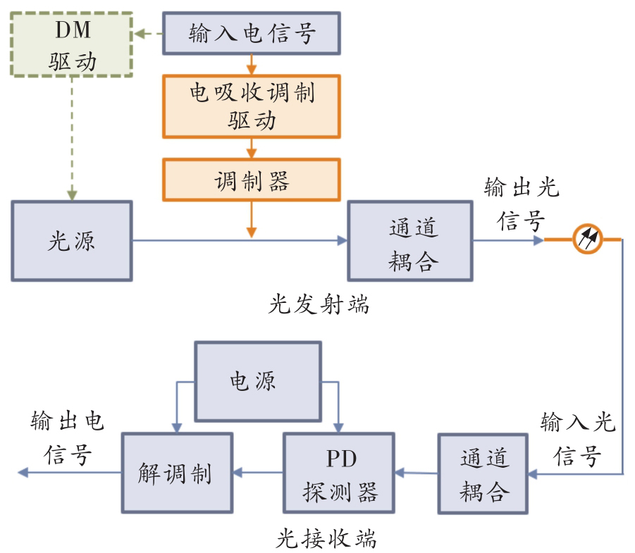
    Fig. 1. The basic principle of the optical module
    Direct modulation optical module link
    Fig. 2. Direct modulation optical module link
    The basic principle of the electrical-optical conversion circuit used in this paper
    Fig. 3. The basic principle of the electrical-optical conversion circuit used in this paper
    Schematic diagram of the equivalent internal circuit of VCSEL
    Fig. 4. Schematic diagram of the equivalent internal circuit of VCSEL
    Transient response curve of laser model
    Fig. 5. Transient response curve of laser model
    The schematic diagram of the PRBS31 differential voltage signal directly driving the VCSEL
    Fig. 6. The schematic diagram of the PRBS31 differential voltage signal directly driving the VCSEL
    The eye diagram of the output optical signal at dif-ferent transmission rates
    Fig. 7. The eye diagram of the output optical signal at dif-ferent transmission rates
    Test schematic diagram of scheme 1
    Fig. 8. Test schematic diagram of scheme 1
    Test schematic diagram of scheme 2
    Fig. 9. Test schematic diagram of scheme 2
    The typical signal eye diagram of the TOSA terminal output in scheme 1
    Fig. 10. The typical signal eye diagram of the TOSA terminal output in scheme 1
    The BER under different differential voltage and bias current driving in scheme 1
    Fig. 11. The BER under different differential voltage and bias current driving in scheme 1
    The eye diagram at the differential voltage of 500 mV and the bias current of 15 mA for scheme 1
    Fig. 12. The eye diagram at the differential voltage of 500 mV and the bias current of 15 mA for scheme 1
    The typical signal eye diagram of the TOSA terminal output in scheme 2
    Fig. 13. The typical signal eye diagram of the TOSA terminal output in scheme 2
    The BER under different differential voltage and bias current driving in scheme 2
    Fig. 14. The BER under different differential voltage and bias current driving in scheme 2
    Variation of S parameters with frequency at two transmission distances
    Fig. 15. Variation of S parameters with frequency at two transmission distances
    参数
    阈值电流Ith/mA1.0
    斜率系数η/mW/mA0.05
    结电容Cj/fF115
    光路等效电阻RVL54
    光路等效电感LVL/nH1.2
    结电阻Rj165
    焊点电容Cp/fF10
    焊点电阻Rp1
    光路等效电容CVL/fF100
    Table 1. 10 Gbit/s VCSEL parameters involved in the simulation model[10]
    电传输距离/mm消光比/dB眼高/μW眼宽/ps光调制幅度/μW
    2002.16~5.5882~14959.1~61.5165~319
    100.84~6.6927~17253.1~73.157~333
    Table 2. The range of eye diagram parameters for the two schemes when the BER is less than 10-12
    Hailong LIAO, Guodong WANG, Hua MIAO, Guoping ZHANG. An Ultra-Low-Power Optical Transmitter for Short-Reach Optical Communication[J]. Study On Optical Communications, 2024, 50(3): 23001001
    Download Citation