
Guangcheng Zhong, Congbiao Lei, Yuxuan Jiang, Liang Xie. Board Level Signal Integrity Study of Ultra-High-Speed Optical Module for Data Centers[J]. Study On Optical Communications, 2024, 50(5): 24003001
- Study On Optical Communications
- Vol. 50, Issue 5, 24003001 (2024)
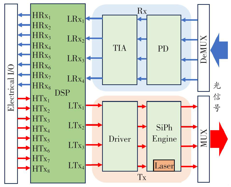
Fig. 1. Basic architecture of the 400 Gbit/s QSFP-DD optical module

Fig. 2. Simulation model and equivalent circuit
Fig. 3. The influence of the radius of each layer back pad of differential hole on the transmission performance
Fig. 4. Simulation model of the inner BGA connection structure
Fig. 5. Influence of inner BGA connection structure anti pad on transmission performance
Fig. 6. Five different anti pad shapes and vias places of the inner BGA connection structure
Fig. 7. 7 SDD21 simulation results of the inner BGA connection structure with five different anti pad shapes and vias places
Fig. 8. Simulation model of optical module PCB high-speed channel
Fig. 9. Mixed-mode S-parameters of 3 groups of high-speed channel on optical module PCB
Fig. 10. Simulated eye diagram results of optical module PCB high-speed channel
Fig. 11. Test platform of optical module
Fig. 12. SDD11 test results of optical module in high speed channel
Fig. 13. Comparison of simulation and test results of impedance distribution in high speed channel of optical module


Set citation alerts for the article
Please enter your email address

© Copyright 2018-2021 | Chinese Laser Press. All Rights Reserved 沪ICP备15018463号-20