- SJ_Zhang
- Mar. 30, 2025
Abstract
Optically bistable materials respond to a single input with two possible optical outputs, contingent on excitation history. Such materials would be ideal for optical switching and memory, but the limited understanding of intrinsic optical bistability (IOB) prevents the development of nanoscale IOB materials suitable for devices. Here we demonstrate IOB in Nd3+-doped KPb2Cl5 avalanching nanoparticles, which switch with high contrast between luminescent and non-luminescent states, with hysteresis characteristic of bistability. We elucidate a non-thermal mechanism in which IOB originates from suppressed non-radiative relaxation in Nd3+ ions and from the positive feedback of photon avalanching, resulting in extreme, >200th-order optical nonlinearities. The modulation of laser pulsing tunes the hysteresis widths, and dual-laser excitation enables transistor-like optical switching. This control over nanoscale IOB establishes avalanching nanoparticles for photonic devices in which light is used to manipulate light.
Main
Optical bistability is a phenomenon in which a material can produce and switch between two different optical responses under a single-input condition1. For example, an optically bistable material can exhibit two different levels of luminescence2, reflectivity3, transmission4 or refractive index5 when excited at the same power and wavelength. The optical behaviour of such materials is characterized by abrupt transitions between two highly stable states, well-defined power thresholds and hysteresis analogous to the flipping of magnetic domains6. Owing to their ability to maintain discrete, photoswitchable and stable states, optically bistable materials hold promise for optical logic, memory7,8 and computing9,10.
For practical application, bistable optical switches must be fast, reproducible, power efficient and readily integrated into dense circuitry. Most reports on optically bistable materials are based on bulk materials or utilize external cavities3,4,11,12, entailing complex architectures and complicating potential device fabrication. Reducing the size of bistable materials below 100 nm would facilitate very large-scale integration and solution-based processing. Such materials would ideally derive their optical bistability from purely electronic processes intrinsic to the host material, rather than poorly controllable thermal effects. However, a limited understanding of the mechanisms for achieving non-thermal intrinsic optical bistability (IOB) has slowed the development of nanoscale IOB.
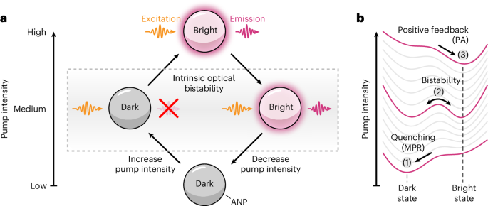
To discover nanoscale IOB materials, we hypothesized that recently described giant nonlinear optical responses of photon avalanching nanoparticles (ANPs)13,14 could provide the positive feedback that is a critical requirement for observing IOB15,16. Although IOB has been previously observed in Ln3+-doped bulk crystals17,18,19,20 and nanoparticles21,22, the mechanisms in these materials were ultimately attributed to uncontrollable thermal phenomena2,23. Here we demonstrate non-thermal IOB in Nd3+-doped KPb2Cl5 nanoparticles and elucidate a mechanism in which IOB is driven by photon avalanches (PA) with extreme nonlinearity orders of s > 200, where the emission intensity Iem scales with the excitation power P as Iem ∝ Ps. These low-phonon-energy ANPs exhibit two luminescent states: a dark, non-emissive state and a bright state that emits upconverted light (Fig. 1a), with the current ANP state determined by its 1,064 nm excitation intensity history. We find that the dark state is stabilized by non-radiative quenching of excited energy levels, and the bright state is stabilized by positive feedback from a PA process (Fig. 1b). By moving between these states and manipulating the hysteresis that controls their bistability, we can efficiently switch ANP luminescence and demonstrate high-contrast, transistor-like optical behaviour.
Fig. 1: IOB in KPb2Cl5:Nd3+ ANPs.
a, Bistable ANPs switch from a dark to a bright, stable state at high 1,064 nm pump intensity, which persists even after the power decreases. ANPs that have not been previously subjected to high intensities show much weaker emission under the same excitation conditions. b, Landscape of ANP states at different pump intensities. Quenching by MPR stabilizes the dark state (1). In contrast, the positive feedback loop of ESA and CR leads to PA and stabilizes the bright state (3). Intermediate excitation intensities result in a double well (2) in which the bistable dark and bright states are separated by a potential energy barrier that gives rise to instability and history dependence.
Results and discussion
Bistable luminescence of ANPs
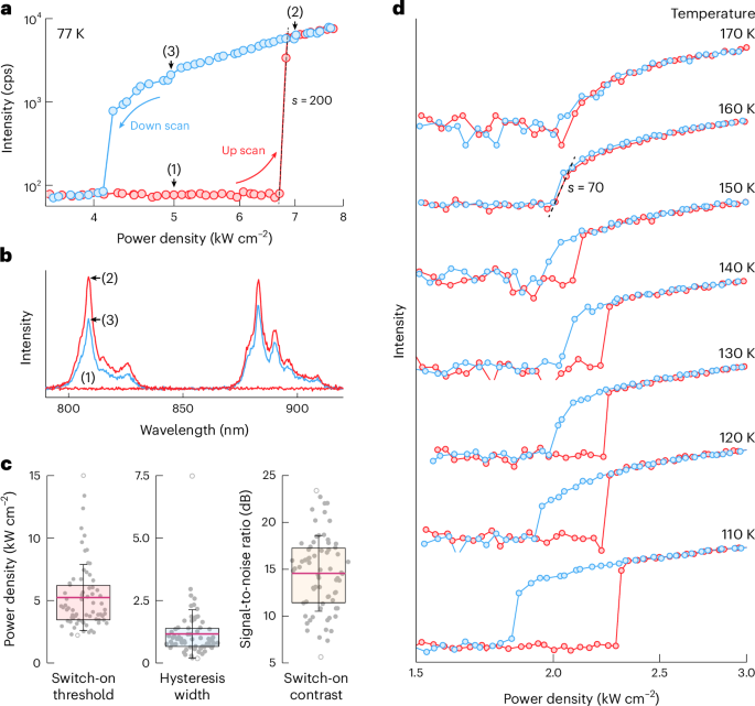
To identify nanomaterials that exhibit extreme optical nonlinearities, and possibly IOB, we explored KPb2Cl5 nanocrystals because their low phonon energies enable PA in Nd3+ dopants at room temperature (synthesis and characterization details are provided in the Supplementary Information). Additionally, the KPb2Cl5 matrix provides chemical stability at both ambient and cryogenic conditions24. We sought to determine if the nonlinearities of these materials would be more pronounced when cooled as the multiphonon relaxation (MPR) rates theoretically decrease by several orders of magnitude at low temperature (Supplementary Fig. 3)25. Liquid-nitrogen-cooled films of KPb2Cl5 nanoparticles doped with 16 mol% Nd3+ show sharp increases in 810 nm emission when the 1,064 nm pump intensity reaches a threshold value of 6.7 kW cm–2 (Fig. 2a). By fitting the linear region of the power-dependent luminescence curve at the switch-on threshold, we measure a slope indicating a nonlinearity of s ≥ 200 (Fig. 2a), constrained by instrumental limitations and an order of magnitude steeper than nonlinear reports of PA at room temperature. Even when stepping pump intensities at the smallest possible increments, we do not detect emission between the discrete dark and bright states. Such discrete jumps may reflect the threshold behaviour of individual ANPs, because the spatial resolution at such extreme nonlinearities is comparable to the size of individual ANPs13,26. These results show that at 77 K, Nd3+-doped KPb2Cl5 nanocrystals exhibit an extreme PA that is a prerequisite for IOB.
Fig. 2: Bistable luminescence of KPb2Cl5:Nd3+ ANPs.
a, Pump power dependence of Nd3+ emission (810 nm, 4F5/2 → 4I9/2) in KPb2Cl5:Nd3+ ANPs at 77 K. The red data points represent the luminescence intensity acquired with increasing excitation intensity (up scan) and blue, with decreasing excitation intensity (down scan). The number indices represent the sequence of events. b, Luminescence spectra of KPb2Cl5:Nd3+ nanocrystals corresponding to power density and scan direction labelled in a by the number indices. c, Switch-on threshold, hysteresis width and switch-on contrast from n = 71 independent measurement spots on a film sample of KPb2Cl5:Nd3+ ANPs. Dots, experimental data points. The box plots display the mean (pink line), standard deviation (whiskers), and 25th and 75th percentiles (box bounds). The minima and maxima are shown as open circles. The measurement parameters are indicated below each box plot. d, Pump power dependence of Nd3+ emission (810 nm, 4F5/2 → 4I9/2) in KPb2Cl5:Nd3+ ANPs in the 110–170 K temperature range. Emission scaling at the switch-on threshold is derived from a linear fit of the log[light–light] curves; see the dashed lines and nonlinearity (s) values in a and d.
Reduction in the pump intensity below the 6.7 kW cm–2 switch-on threshold does not reduce the ANP emission much until the irradiance decreases to 4.2 kW cm–2, at which point the ANPs abruptly turn dark (Fig. 2a). This non-zero difference between the excitation intensity required to switch the ANPs on and off creates a hysteresis in their optical response, indicating optical bistability. Within this bistable region, the two stable states of the ANPs are manifested as dark or bright emission at intermediate pump intensity (for example, 5 kW cm–2), depending on whether the luminescence is measured before or after reaching the switch-on threshold. Such bistability is spectrally observed in multiple Nd3+ emission lines, including the 810 nm (4F5/2 → 4I9/2) and 880 nm (4F3/2 → 4I9/2) transitions (Fig. 2b).
We observed this luminescence hysteresis on two different optical setups (Supplementary Fig. 4) and on different substrates (Supplementary Fig. 5). Furthermore, when we varied the acquisition dwell times (0.1–10 s) used for each pump power, the hysteresis widths and thresholds remained constant (Supplementary Fig. 6), indicating that the hysteresis does not originate from time-dependent factors such as laser-induced heating or slow PA rise times (~20 ms; Supplementary Fig. 21). Even room-temperature rise times (50–70 ms)24 are shorter than the shortest dwell times (0.1 s), ensuring that samples are measured at steady state. All of these observations support our conclusion that the ANP emission signal is intrinsically bistable and not the result of experimental artefacts27.
To obtain statistical information about the reproducibility of IOB and characteristics including the switch-on threshold, hysteresis width and intensity contrast, we measured the pump power dependence at multiple spots across a film of KPb2Cl5:Nd3+ ANPs (Supplementary Fig. 7 and Fig. 2c). The average switch-on power density is 5.2 kW cm–2, corresponding to 64 μW, suitable for low-power requirements (microwatts to milliwatts) in optical computing28. On average, the width of luminescence hysteresis is 1 kW cm–2, and the photoswitching contrast of the KPb2Cl5:Nd3+ ANPs (that is, signal-to-noise ratio at the switch-on threshold) is 14 ± 4 dB, sufficiently high to unambiguously differentiate between the bright and dark ANP states29. This contrast is one to two orders of magnitude greater than that of previously reported IOB nanomaterials, which were studied at room temperature (Supplementary Table 2 provides a comparison of KPb2Cl5:Nd3+ ANPs to other optically bistable materials).
To demonstrate the stability and reproducibility of this IOB, we repeated the optical hysteresis measurements on the same spot (Fig. 2a) 100 times over 12 h (Supplementary Fig. 8). Despite minor variations in the switch-on threshold (6.52 ± 0.21 kW cm–2) and hysteresis width (2.20 ± 0.15 kW cm–2), possibly due to sample drift, the IOB is consistently observed for every cycle. Notably, these ANPs show no photodarkening or blinking30,31.
To probe how these nanocrystals give rise to IOB, we varied their Nd3+-doping levels. High nonlinearity and luminescence hysteresis are predominantly observed in samples with Nd3+ concentrations above 4 mol% (Supplementary Fig. 9), suggesting that the nonlinearity requisite for the IOB is driven by a mechanism such as PA that incorporates distance-dependent energy transfer processes13,32. To understand the role of the host matrix, we measured the luminescence power dependence of Nd3+ ions doped in a higher-phonon-energy host, NaYF4. However, we do not observe PA or luminescence hysteresis even when NaYF4:Nd3+ nanocrystals are cooled to 8 K (Supplementary Fig. 10), underscoring the need for low-phonon-energy hosts to suppress MPR and observe PA and IOB. Thus, cryogenic temperatures alone are insufficient to promote IOB from nonlinear Nd3+ luminescence.
We further investigated the impact of thermal phonons on the quenching of Nd3+ energy levels (for example, 4I11/2) by measuring the power-dependent luminescence of KPb2Cl5:Nd3+ ANPs at different temperatures. We find that higher temperatures lead to a lower degree of nonlinearity and narrowing of luminescence hysteresis (Fig. 2d), making thermal contributions to IOB unlikely. Importantly, we observe IOB at temperatures as high as 150 K (Fig. 2d). The switch-on threshold also shifts to lower power densities with increasing temperatures, correlating with an enhanced phonon-assisted ground-state absorption (GSA). In particular, at 160 K, ANPs do not show luminescence hysteresis despite their highly nonlinear (s = 70) luminescence, suggesting that extreme nonlinearities (s ≥ 100) are required to induce IOB in KPb2Cl5:Nd3+ ANPs.
Mechanism of IOB in ANPs
To corroborate these experimental results and better understand this observed IOB, we used a differential rate equation model33 to numerically simulate the time-dependent population of the 4fN energy levels of Nd3+ ions in a KPb2Cl5 host (Supplementary Note 1). Our simulations reproduce the nonlinear power scaling of KPb2Cl5:Nd3+ luminescence and, most importantly, the luminescence hysteresis of experimental observations (Supplementary Fig. 11). Similar results were also found using a simplified rate equation model (Supplementary Note 2). These simulations do not incorporate thermal phenomena, highlighting that IOB in KPb2Cl5:Nd3+ ANPs is governed only by the optical activation of electronic 4f energy levels, which distinguishes this system from thermal IOB in other materials19,23.
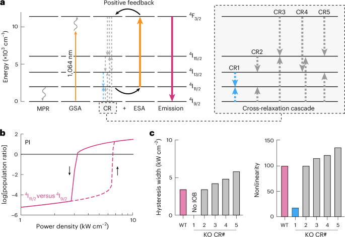
The photophysical mechanism (Supplementary Fig. 13) extracted from these simulations33 resembles the canonical PA process in which excited-state absorption (ESA; Fig. 3a, thick orange arrow) dominates over GSA (thin orange arrow) and couples to a cascade of cross-relaxation (CR) processes (dashed arrows, CR1–5) to form an ‘energy loop’13. Each CR process multiplies the population of low-lying excited manifolds of Nd3+ ions, like 4I11/2, increasing the rates of ESA and CR from those levels. Repeated CR + ESA amplifies those populations exponentially in a positive feedback loop, resulting in the observed nonlinear behaviour.
Fig. 3: Model of IOB in KPb2Cl5:Nd3+ ANPs.
a, Simplified energy-level diagram of Nd3+ ions showing GSA, CR, ESA and emission. ESA and a collection of CR processes (CR1-5) form a positive feedback loop, leading to giant signal amplification and IOB. Competing MPR (wavy arrow) is also shown. b, Pump power dependence of Nd3+ excited (4I11/2) versus ground (4I9/2) energy-level population ratio in a simulated KPb2Cl5:20 mol% Nd3+ system. The dashed line corresponds to the power-up scan and the solid line to the power-down scan. c, Influence of CR pathway knock-outs (KOs) on the hysteresis width and nonlinearity for 4F3/2 → 4I9/2 radiative transition. WT, wild type; CR#, CR1-5 as shown in a.
Such looping is supported by our observation that simulated populations of the Nd3+ ground (4I9/2) and first-excited (4I11/2) 4f electronic levels are inverted at the switch-on pump threshold (Fig. 3b). In particular, this population inversion (PI) is maintained even when the power is reduced below that threshold, resulting in hysteresis in the power dependence of the population ratio between the 4I11/2 and 4I9/2 energy levels. The PI is correlated with the emergence of the bright state of ANPs, suggesting that bright and dark steady states of these bistable ANPs are distinguished by their inverted and non-inverted excited-level populations, respectively.
To identify the critical transitions responsible for IOB, we performed a series of ‘knock-out’ simulations in which we systematically deactivate individual CR pathways in the CR cascade (CR1–5) that drives the PA (additional knock-out methods and results provided in the Supplementary Information)34. When MPR and other parameters are held constant, the simulated power-dependent luminescence of the knock-out systems reveals that among the CR processes, CR1 (Fig. 3a; [(4I9/2 → 4I11/2):(4I13/2 → 4I11/2)]) has the most impact on the performance of bistable ANPs. Deactivating CR1 reduces the nonlinearity by 5.8-fold (to s = 17) and eliminates luminescence hysteresis (Fig. 3c). Although CR processes from the 4F3/2 excited energy level (Fig. 3a, CR3–5) are not essential to establish PI, knocking them out shifts the switch-on threshold to higher values (Supplementary Fig. 11). We believe that these pathways are needed to repopulate the lower Nd3+ energy levels (4I11/2, 4I13/2 and 4I15/2) after photon absorption and they contribute to the nonlinear behaviour of ANPs through a CR cascade. Finally, we compared the rate of CR1 in the wild-type (no knock-outs) KPb2Cl5:Nd3+ with that of other transitions. We find that within the bistable region of luminescence, the 4I11/2 energy level is populated via CR1 faster than it is depopulated via MPR (Supplementary Figs. 14 and 15). This dominance of CR1 over quenching processes appears to be a necessary condition for IOB, which is satisfied in low-phonon-energy matrices that result in low MPR rates (Supplementary Table 4).
On the basis of these mechanistic observations, we construct a conceptual scheme explaining how IOB occurs in KPb2Cl5:Nd3+ ANPs (Fig. 1b). These bistable ANPs exhibit two stable macroscopic states: (i) a dark, non-emissive state with Nd3+ ions occupying their ground energy level and (ii) an avalanching, luminescent state with Nd3+ ions populated predominantly in their first-excited energy level. At low 1,064 nm pump intensities (Fig. 1b, Plow), the dark state (Fig. 1b, (1)) is stabilized from moderate increases in pump power by the suppression of non-resonant GSA in the low-phonon-energy KPb2Cl5 host at low temperatures. MPR also stabilizes the dark state by quenching the few excited Nd3+ ions before they can achieve the intermediate 4I11/2 populations necessary for avalanching. The bright state (Fig. 1b, (3))—established at high intensities (Phigh)—is stable because the positive feedback of the avalanching process maintains PI. Even when the pump power is reduced below the PA threshold, avalanching persists because the intermediate 4I11/2 population has already been seeded and is not readily quenched due to suppressed MPR in the low-phonon-energy host. Owing to the giant nonlinearity of PA, only a small amount of ESA from this 4I11/2 level is necessary to sustain the cascade of CR back to the same level and counteract its depopulation by MPR. As a result, both bright and dark states are stable at moderate pump intensities (Fig. 1b, (2), Pmed).
To reiterate, this IOB is a direct consequence of the low phonon energy of KPb2Cl5 and the positive feedback of PA in Nd3+ dopants. These driving forces create a potential energy barrier (that is, instability region) that separates the two states in the bistable regime (the potential energy surface is shown in Fig. 1b). This barrier ultimately gives rise to the latching hysteresis and history dependence that characterizes the bistable luminescence of KPb2Cl5:Nd3+ ANPs.
Temporal modulation of IOB
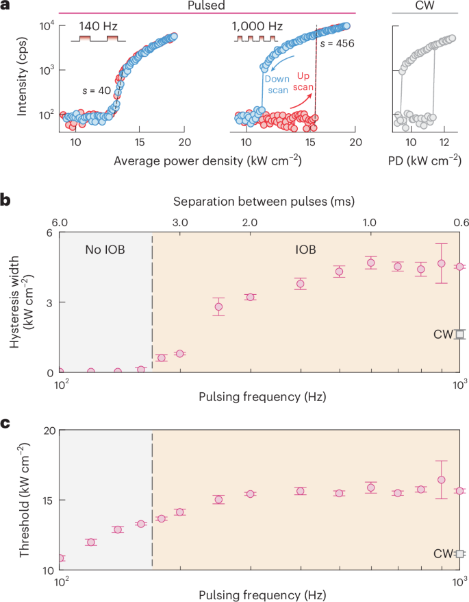
After establishing that IOB in KPb2Cl5:Nd3+ ANPs is realized through a PA mechanism, we hypothesized that the dynamics of this positive feedback could be manipulated by modulating the excitation power over time, potentially influencing the IOB behaviour. To test this hypothesis, we performed power dependence studies with a 1,064 nm pump modulated at various pulse frequencies and duty cycles. We find that modulating the laser selectively inhibits or induces IOB in ANPs and allows for control over luminescence hysteresis (Fig. 4 and Supplementary Figs. 16 and 17). Slow pulsing (<170 Hz, 40% duty cycle) of the excitation laser eliminates the hysteresis observed with continuous-wave (CW) 1,064 nm excitation and decreases the PA nonlinearity (s = 40 at 140 Hz; Fig. 4a). In contrast, at higher pulsing frequencies the hysteresis widens (Fig. 4b), and the PA threshold shifts to higher average powers (Fig. 4c). At a 1,000 Hz pump frequency, the hysteresis width reached 4.5 kW cm–2 (Fig. 4) and 24 kW cm–2 (Supplementary Fig. 18) for 40% and 10% pulse duty cycle, respectively, considerably wider than that under CW excitation (1.6 kW cm–2).
Fig. 4: Temporal modulation of luminescence hysteresis.
a, Pump power dependence of Nd3+ emission in KPb2Cl5:Nd3+ ANPs at 77 K under 1,064 nm CW and pulsed pump excitation (40% duty cycle). cps, counts per second; PD, power density. b,c, Hysteresis width (b) and PA switch-on threshold versus pump pulse frequency (40% duty cycle) (c). The corresponding dependence on the temporal separation between pulses is also shown. The respective values under the CW pump are shown as squares. Emission scaling in a is derived from a linear fit of the log[light–light] curves. Data in b and c are shown as the mean values ± one standard deviation (n = 3).
We rationalize this dynamic control over IOB by considering the pulse duration and period between pulses. The greater switch-on power thresholds at higher frequencies arise due to the decreased probability of GSA with decreasing pulse energies (25 nJ at 100 Hz versus 3.6 nJ at 1,000 Hz). Similarly, IOB emerges at high pulsing frequencies because the time period between pulses is short enough to sustain the positive feedback of CR + ESA in KPb2Cl5:Nd3+ ANPs. We also examined the notable difference in hysteresis characteristics between CW and high-frequency pulsed excitation of ANPs. The widening of hysteresis and higher average switch-on powers observed in the 500–1,000 Hz range are not observed at pulse frequencies higher than 4,000 Hz because such closely spaced pulses become analogous to quasi-CW excitation (Supplementary Figs. 19 and 20). On the basis of the frequencies at which ANPs begin to exhibit luminescence hysteresis (180 Hz and 300 Hz at 40% and 10% duty cycle, respectively), we estimate that the PI in ANPs lasts up to 3 ms, which is probably related to the lifetime of the 4I11/2 excited energy level of Nd3+ ions in KPb2Cl5 matrix (2.3 ms at room temperature35). The duration of PI also dictates the photoactivation kinetics of the KPb2Cl5:Nd3+ ANPs. With high-frequency pulsing, we measure short rise times for emitting energy levels populated directly by ESA (for example, 4F3/2 is populated in 305 µs). In contrast, PI is lost between low-frequency excitation pulses, resulting in millisecond rise times from the initially slow GSA followed by PA, similar to KPb2Cl5:Nd3+ ANPs at room temperature24 (Supplementary Note 3).
The fact that this IOB occurs via photophysical interactions between dopant ions (that is, non-thermally) allows us to actively control the switch-on power threshold, hysteresis width and nonlinearity of bistable ANPs, underscoring their utility in photonic applications36,37,38.
Optical switching via instability crossing
With the ability to induce and control IOB in KPb2Cl5:Nd3+ ANPs, we sought to demonstrate how their bistable response can be used for switching logic and memory. In principle, a bistable ANP can be treated as a bit whose dark state (assigned a value of 0) may be flipped by increasing the pump intensity to activate the ANP’s bright (1) state. The bright bit can then be maintained at lower pump intensities. However, this single-laser approach may be impractical as it requires varying the pump intensity and requires a dedicated laser beam to address each bit independently.
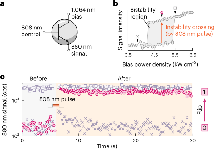
To overcome these challenges, we hypothesized that bistable ANPs could be manipulated using laser pumps at two different wavelengths, mimicking a transistor (Fig. 5a). We developed an approach that uses an 808 nm control laser pulse to set an ANP in its bright state and a constant 1,064 nm laser as a bias to maintain this state. The advantage of this two-laser approach is that the 1,064 nm bias laser, in principle, can be spread diffusely to maintain the state of many bits simultaneously, allowing the control laser to raster freely and flip individual bits. Furthermore, the 808 nm control pulse enables the fast switching of ANPs from their dark to a bright state because it is resonant with GSA (4I9/2 → 4F3/2) in Nd3+ ions. This resonant excitation of the ANP bright states at 808 nm bypasses, or crosses, the instability barrier that normally exists when exciting ANPs non-resonantly at 1,064 nm (Fig. 5b). Such ‘instability crossing’ simplifies bit operations because it eliminates the need to vary the 1,064 nm laser power.
Fig. 5: Photoswitching of ANPs via instability crossing.
a, Schematic of the transistor-like addressing of KPb2Cl5:Nd3+ nanocrystals with 808 nm control input (7 W cm–2) under a constant 1,064 nm pump bias (4.7 kW cm–2). b, Pump power dependence of KPb2Cl5:Nd3+ nanocrystals used for photoswitching experiments. The bistability region (grey) and instability crossing (orange arrow) are shown. The 1,064 nm bias for the experiment in c was applied at three different power densities: a dark state outside the bistability region (cross), within the bistability region (circle) and a bright state outside the bistability region (square). c, Time recording of emission at 880 nm of KPb2Cl5:Nd3+ ANPs before and after 808 nm control pulse when biased at 1,064 nm pump. The symbols in c indicate the 1,064 nm bias power densities for each trace as defined by the placement of those symbols in b.
When we implemented this two-laser scheme on a film of ANPs, we observed that their 880 nm (4F3/2 → 4I9/2) luminescence flips from a dark (0) to a bright (1) state after an ~1 s pulse of the 808 nm laser and is maintained as long as a 1,064 nm bias laser (4.7 kW cm–2) is present (Fig. 5c). In particular, the switching between the two stable states is achieved at an extremely low 808 nm power density (7 W cm–2, corresponding to 75 nW power). We note that the latching of the bright state via instability crossing would not occur with thermally activated avalanching and is enabled by the PA-driven IOB in KPb2Cl5:Nd3+ ANPs.
To determine whether photoswitching occurs only when ANPs are biased within the bistable region, we performed control experiments by applying the 1,064 nm laser bias outside the bistable region and observed no change in ANP luminescence before or after the 808 nm input (Fig. 5c). Furthermore, we demonstrate the instability crossing using a pulsed 1,064 nm laser to exploit larger hysteresis (Supplementary Fig. 22) and using control lasers with wavelengths resonant with different GSA transitions of Nd3+ ions (875 nm for 4I9/2 → 4F3/2 GSA and 745 nm for 4I9/2 → 4F7/2 GSA; Supplementary Fig. 23). These findings demonstrate the versatility of bistable ANPs and establish the foundation for their use as nanoscale optical transistors and volatile optical memory39.
Conclusion
Our findings demonstrate the realization of purely optical, nonlinear and intrinsically bistable luminescence in KPb2Cl5:Nd3+ nanocrystals. This behaviour is realized by suppressing phonon-mediated transitions and through the positive feedback of PA among Nd3+ dopants. Unlike other Ln3+-doped materials that exhibit IOB, in KPb2Cl5:Nd3+ ANPs, IOB arises from a non-thermal mechanism quantitatively explained by photophysical modelling. The lack of thermal contribution to IOB in our model is supported by multiple lines of experimental evidence, including (1) the continued observation of IOB at low duty cycles, the insensitivity of the hysteresis to (2) variations in scan rate or (3) the thermal conductivity of the substrate, and (4) the ability to photoswitch bistable particles with a low-power laser. These observations—discussed in greater detail in Supplementary Discussion 1—are fully consistent with an all-optical mechanism for IOB and are difficult to reconcile with thermally mediated bistability.
The all-optical nature of IOB in KPb2Cl5:Nd3+ ANPs allows the tuning of luminescence hysteresis characteristics, optical switching and memory. IOB-based switching of KPb2Cl5:Nd3+ ANPs is complementary to—but distinct from—the previously reported photoswitching of NaYF4:Tm3+ ANPs. Although the photodarkening of Tm3+-doped ANPs occurs through the formation of long-lived defects akin to persistent memory, IOB-based photoswitching is a dynamic process analogous to volatile memory39, as we demonstrate here. We envision that bistable ANPs can address several challenges that currently limit the construction of digital optical logic gates, such as cascadability, logic-level restoration and the absence of critical biasing10,40. Combined with solution processing and direct lithography methods, the three-dimensional volumetric interconnects of bistable ANPs could be fabricated for high-density optical computing10,41. Furthermore, bistable ANPs can be operated with low-power, cost-efficient lasers compatible with telecommunication wavelengths or silicon detectors, facilitating integration with existing technologies. These bistable ANPs are analogous to nanoscale optical transistors, paving the way for general-purpose digital optical computing, neuromorphic circuitry, imaging and related photonic technologies.
Methods
All the experimental details, including the synthesis of nanocrystals, structural characterization, optical measurements and simulations, are provided in the Supplementary Information.
Journal
Mar. 30, 2025

