• Journal of Inorganic Materials
  • Vol. 35, Issue 2, 199 (2020)
Tong ZHANG, Zi-Juan LI, Ze-Kun GUO, Yan TIAN..., Hao-Jian LIN, Ning-Sheng XU, Jun CHEN, Shao-Zhi DENG* and Fei LIU*|Show fewer author(s)
Author Affiliations
  • Guangdong Key Laboratory of Display Materials and Technologies, State Key Laboratory of Optoelectronic Materials and Technology, School of Eletronics and Information Technology, Sun Yat-sen University, Guangzhou 510275, China
  • show less
    DOI: 10.15541/jim20190070 Cite this Article
    Tong ZHANG, Zi-Juan LI, Ze-Kun GUO, Yan TIAN, Hao-Jian LIN, Ning-Sheng XU, Jun CHEN, Shao-Zhi DENG, Fei LIU. Single Crystalline SmB6 Nanostructure Arrays: Controllable Synthesis and Field Emission Property[J]. Journal of Inorganic Materials, 2020, 35(2): 199 Copy Citation Text show less
    (a, b) Typical low- and high-resolution SEM images of the SmB6 nanowires with inset showing typical side-view image of SmB6 nanowires, and (c, d) side- and top-view images of the SmB6 nanobelts with inset in (c) showing representative high-magnification SEM image of the SmB6 nanobelt
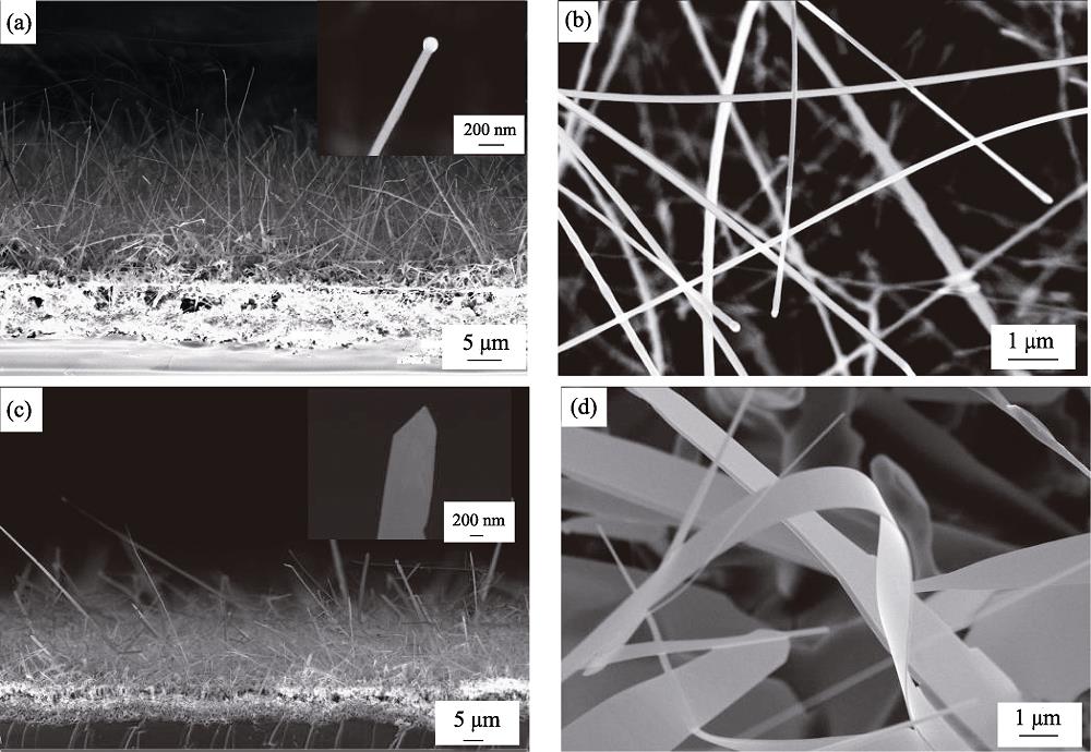
    1. (a, b) Typical low- and high-resolution SEM images of the SmB6 nanowires with inset showing typical side-view image of SmB6 nanowires, and (c, d) side- and top-view images of the SmB6 nanobelts with inset in (c) showing representative high-magnification SEM image of the SmB6 nanobelt
    (a) Typical XRD patterns and (b) Raman spectra of SmB6 nanobelts and nanowires
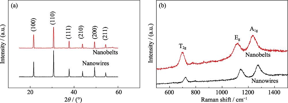
    2. (a) Typical XRD patterns and (b) Raman spectra of SmB6 nanobelts and nanowires
    (a, b) Low- and high-resolution TEM images of the SmB6 nanobelt with inset in (b) showing the corresponding SAED pattern, and (c, d) low- and high-magnification TEM images of the SmB6 nanowire with inset in (d) showing the corresponding SAED pattern
    3. (a, b) Low- and high-resolution TEM images of the SmB6 nanobelt with inset in (b) showing the corresponding SAED pattern, and (c, d) low- and high-magnification TEM images of the SmB6 nanowire with inset in (d) showing the corresponding SAED pattern
    (a) J-E characteristics of the SmB6 nanowires and nanobelts and their corresponding (b) FN plots
    4. (a) J-E characteristics of the SmB6 nanowires and nanobelts and their corresponding (b) FN plots
    MorphologyDensity/cm-2Length/μmMean length/μmMean top diameter/nmAspect radioSpecific surface area/μm-1
    SmB6 nanowires5×10720-12047.810844218.5
    SmB6 nanobelts4×10710-9036.37647739.6
    Table 1. Morphological parameters of the SmB6 nanowires and nanobelts
    MaterialMeasurementAreas of samples/cm2Eon/(V·μm-1)Jmax/(μA·cm-2)Field enhancement factor, β
    SmB6 nanowiresTransparent anode method1565.71461
    SmB6 nanobeltsTransparent anode method13.24466.161921
    SmB6 nanowires[14]Transparent anode method0.496.5306996
    SmB6 nanopencils[14]Transparent anode method0.26.92371150
    SmB6 nanowires[15]Transparent anode method0.7852.7-4.2-2207-4741
    LaB6 nanowires[8]Transparent anode method-1.8257001072
    Carbon nanotubes[21]Transparent anode method0.00383.22.184×106768-956
    ZnO nanobelts[22]Anode probe method-6.640170700
    Table 2. Comparison of field emission properies of some excellent cathode nanostructures
    Tong ZHANG, Zi-Juan LI, Ze-Kun GUO, Yan TIAN, Hao-Jian LIN, Ning-Sheng XU, Jun CHEN, Shao-Zhi DENG, Fei LIU. Single Crystalline SmB6 Nanostructure Arrays: Controllable Synthesis and Field Emission Property[J]. Journal of Inorganic Materials, 2020, 35(2): 199
    Download Citation