• Infrared and Laser Engineering
  • Vol. 54, Issue 2, 20240441 (2025)
Chonghao GAN1, Wenlin FENG1,2, Xiangzhi LIU1,2,3, Xiaozhan YANG1,2,3..., Xiangmeng LU3, Dajian CUI3 and Cong CHEN4|Show fewer author(s)
Author Affiliations
  • 1School of Science, Chongqing University of Technology, Chongqing 400054, China
  • 2Chongqing Key Laboratory of New Storage Energy Materials and Devices, Chongqing 400054, China
  • 3Chongqing Key Laboratory of Quantum Information Chips and Devices, Chongqing 400061, China
  • 4School of Electrical Engineering, Tongling University, Chinese Academy of Sciences, Tongling 244061, China
  • show less
    DOI: 10.3788/IRLA20240441 Cite this Article
    Chonghao GAN, Wenlin FENG, Xiangzhi LIU, Xiaozhan YANG, Xiangmeng LU, Dajian CUI, Cong CHEN. Progress in analysis of large field of view achromatic function and zoom technology of metalenses (cover paper)[J]. Infrared and Laser Engineering, 2025, 54(2): 20240441 Copy Citation Text show less
    Large field of view, achromatic, zoom metalenses
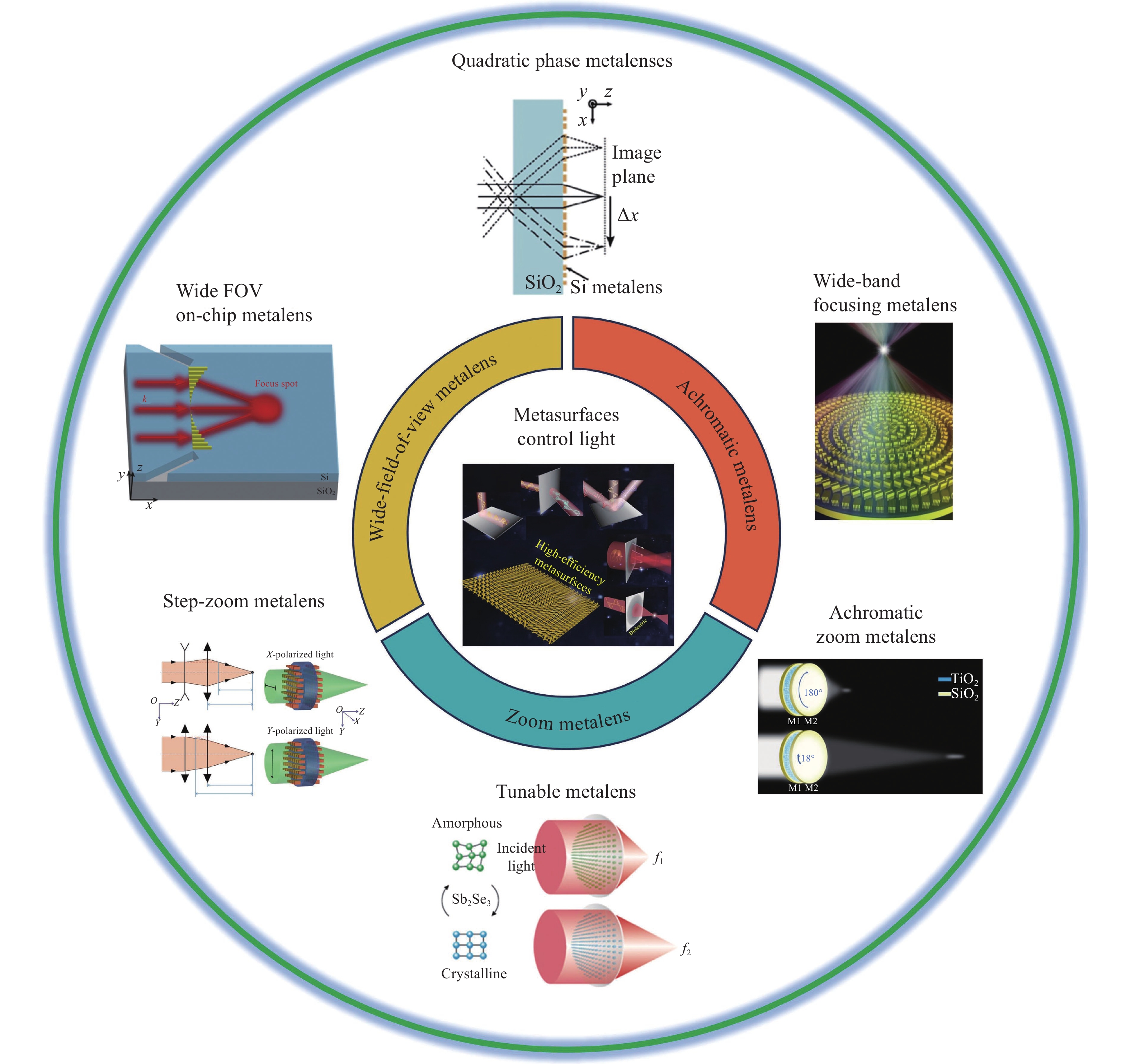
    Fig. 1. Large field of view, achromatic, zoom metalenses
    Generalized Fresnel's law optical path diagram[3]
    Fig. 2. Generalized Fresnel's law optical path diagram[3]
    (a) The incident light is x-polarized light, and the stepping zoom metalens is focused on the pattern[14]; (b) The incident light is y-polarized light, and the step zoom metalens is focused on the lens[14]; (c) On-chip wide FOV metalenses[10]
    Fig. 3. (a) The incident light is x-polarized light, and the stepping zoom metalens is focused on the pattern[14]; (b) The incident light is y-polarized light, and the step zoom metalens is focused on the lens[14]; (c) On-chip wide FOV metalenses[10]
    (a) Structural diagram of a perpendicular curve light field metalens[35]; (b) Focus diagram of perpendicular curve light field metalens[35]; (c) Ray trajectories through the lens[35]; (d) Focusing diagram of metalenses based on the surface of disordered media[36]; (e) Focus view of a single-layer large-field metalens in the mid-infrared band[37]; (f) Light intensity distribution of a single-layer large-field metalens in the mid-infrared band along the z-axis[37]
    Fig. 4. (a) Structural diagram of a perpendicular curve light field metalens[35]; (b) Focus diagram of perpendicular curve light field metalens[35]; (c) Ray trajectories through the lens[35]; (d) Focusing diagram of metalenses based on the surface of disordered media[36]; (e) Focus view of a single-layer large-field metalens in the mid-infrared band[37]; (f) Light intensity distribution of a single-layer large-field metalens in the mid-infrared band along the z-axis[37]
    Device architecture and metalens fabrication[38]. (a) Schematic of the optical setup for MIID; (b) Photograph of the highly compact MIID; (c) Top-view optical microscope image and side-view SEM image of the fabricated
    Fig. 5. Device architecture and metalens fabrication[38]. (a) Schematic of the optical setup for MIID; (b) Photograph of the highly compact MIID; (c) Top-view optical microscope image and side-view SEM image of the fabricated
    (a) Three layer metal metasurface structure [43]; (b) Metal metalenses for color imaging demonstration[43]; (c) Focus view of a metal metalens[43]; (d) Focus view of a multi-region metalens [44]; (e) Focus view of a graphene oxide metalens[45]
    Fig. 6. (a) Three layer metal metasurface structure [43]; (b) Metal metalenses for color imaging demonstration[43]; (c) Focus view of a metal metalens[43]; (d) Focus view of a multi-region metalens [44]; (e) Focus view of a graphene oxide metalens[45]
    (a) Focusing diagram of a metalens of complementary structure and its imaging[46]; (b) Focus diagram of an elliptical cylindrical metalens[48]; (c)Focus diagram of a hexagonal structure metalens[49]; (d) Focus diagram of a rectangular structure metalens[51]
    Fig. 7. (a) Focusing diagram of a metalens of complementary structure and its imaging[46]; (b) Focus diagram of an elliptical cylindrical metalens[48]; (c)Focus diagram of a hexagonal structure metalens[49]; (d) Focus diagram of a rectangular structure metalens[51]
    (a) Metalenses anisotropic nanostructured for imaging of resolution test maps of the USAF[53]; (b) Focus diagram of an anisotropic nanostructured metalens[53]; (c) Structural diagram of mid-infrared achromatic metalens[54]; (d) Mid-infrared achromatic metalens focus diagram[54]; (e) Structural diagram of Longwave infrared achromatic metalens[54]; (f) Longwave infrared achromatic metalens focus diagram[54]; (g) Schematic diagram of the odd-ring metalens and the combined metalens and their corresponding light intensity along the z-axis[56]; (h) Multi-region metalens focus diagram[56]
    Fig. 8. (a) Metalenses anisotropic nanostructured for imaging of resolution test maps of the USAF[53]; (b) Focus diagram of an anisotropic nanostructured metalens[53]; (c) Structural diagram of mid-infrared achromatic metalens[54]; (d) Mid-infrared achromatic metalens focus diagram[54]; (e) Structural diagram of Longwave infrared achromatic metalens[54]; (f) Longwave infrared achromatic metalens focus diagram[54]; (g) Schematic diagram of the odd-ring metalens and the combined metalens and their corresponding light intensity along the z-axis[56]; (h) Multi-region metalens focus diagram[56]
    (a) Schematic diagram of Ge2Se2Te5 metalens[64]; (b) Focusing diagram Ge2Se2Te5 metalens[64]; (c) Schematic diagram of Sb2Se3 metalens[13]; (d) Focusing diagram based on Sb2Se3 metalens[13]
    Fig. 9. (a) Schematic diagram of Ge2Se2Te5 metalens[64]; (b) Focusing diagram Ge2Se2Te5 metalens[64]; (c) Schematic diagram of Sb2Se3 metalens[13]; (d) Focusing diagram based on Sb2Se3 metalens[13]
    (a) Focusing diagram of a large chromatic aberration dispersion zoom metalens[65]; (b) Large chromatic aberration dispersion zoom metalens imaging test for USAF resolution test diagram[65]; (c) Structural diagram of a double-layer metasurface zoom lens[67]; (d) Comparison of theoretical and actual focal lengths at different rotation angles of metasurfaces[67]
    Fig. 10. (a) Focusing diagram of a large chromatic aberration dispersion zoom metalens[65]; (b) Large chromatic aberration dispersion zoom metalens imaging test for USAF resolution test diagram[65]; (c) Structural diagram of a double-layer metasurface zoom lens[67]; (d) Comparison of theoretical and actual focal lengths at different rotation angles of metasurfaces[67]
    DeviceWavelength/nmFocal length/μmFocus on efficiencyNAFOV/(°)
    Step-zoom metalens[14]65840-8023.07%-35.10%0.3-0.1640
    Wide FOV on-chip metalens[10]15503068%120
    Perpendicular curve light field metalenses[35]1.58×1078.75×104>80%0.89120
    Disordered media surface metalenses[36]532160
    wide FOV single-layer metalenses in the mid-infrared[37]3800-4200255%-15%0.85160
    Wide FOV metalens for CMOS image sensors[39]106410083.6%1.6540
    Table 1. Review of the performance of wide FOV metalenses
    DeviceWavelength/μmFocal length/μmFocus on efficiencyNA
    Three-layer metal achromatic metalens[43]0.450.550.651 × 1065.8%-8.7%
    RGB-achromatic metalens[44]0.4880.5320.6581 × 10668%0.7
    Graphene Oxide metalens[45]0.450.550.651000.894
    Achromatic metalens in the visible[46]0.40-0.6623540%0.15
    High-NA and broadband achromatic metalens in the visible[48]0.53-0.85436.4%0.564
    High-NA and broadband achromatic metalens in longwave infrared[49]9-115020.06%0.79
    Broadband achromatic metalens in mid-IR range[51]4-5105-11651.6%0.396-0.430
    Mid-infrared achromatic metalens[53]3-515026.6%-23.0%0.32
    Longwave infrared achromatic metalens[53]8-1415026.4%-41.7%0.55
    Multi-zone achromatic metalens[54]0.43-0.7510035%-63%0.255
    Anisotropic nanostructured metalens[56]0.46-0.70670.2
    Table 2. Review of the performance of achromatic metalenses
    DeviceZoom factorMaterialWavelength/μmFocal length/μmFocus on efficiencyNA
    Linear-polarization-multiplexing metalens [62]Horizontally polarized lightSilicon10.68 × 10672%0.45
    Vertically polarized light40 × 10677%0.1
    LC metalens[63]Change the arrangement of LC moleculesLC0.651040
    4570
    GST metalens[64]AmorphousGe2Se2Te50.38 × 1067 × 106
    Crystalline10 × 106
    Sb2Se3 metalens[13]AmorphousSb2Se31.55415.7%
    Crystalline1233%
    Dispersive zoom metalenses[65]Chromatic dispersionGaN0.45-0.66102.70.78
    69.2
    Rotation zoom metalenses[67]Rotation angle: 0°TiO20.53225.980.5
    Rotation angle: 90°11.250.8
    Table 3. Review of the performance of zoom metalenses
    Chonghao GAN, Wenlin FENG, Xiangzhi LIU, Xiaozhan YANG, Xiangmeng LU, Dajian CUI, Cong CHEN. Progress in analysis of large field of view achromatic function and zoom technology of metalenses (cover paper)[J]. Infrared and Laser Engineering, 2025, 54(2): 20240441
    Download Citation