
Bing Xiong, Mingwei Sun, Changzheng Sun, Zhibiao Hao, Jian Wang, Lai Wang, Yanjun Han, Hongtao Li, Lin Gan, Yi Luo. Waveguide Uni‐Traveling Carrier Photodetectors with Wide Bandwidth and High Responsivity (Invited)[J]. Chinese Journal of Lasers, 2025, 52(5): 0501005
- Chinese Journal of Lasers
- Vol. 52, Issue 5, 0501005 (2025)
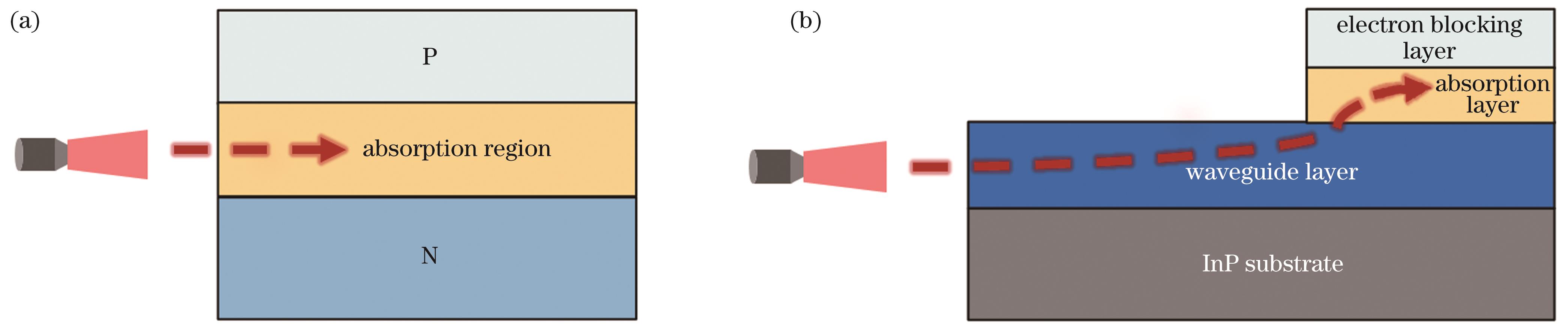
Fig. 1. Schematics of waveguide photodetectors. (a) Simple side-illuminated waveguide photodetector; (b) evanescently coupled waveguide photodetector
![Schematics of evanescently coupled waveguide photodetectors integrated with spot size converter structure. (a) Waveguide photodetector integrated with tapered spot size converter (length of tapered waveguide is shortened proportionally)[19]; (b) waveguide photodetector integrated with dual-stage tapered spot size converter[17]; (c) waveguide photodetector integrated with laterally tapered twin-waveguide structure[20]](/richHtml/zgjg/2025/52/5/0501005/img_02.jpg)
Fig. 2. Schematics of evanescently coupled waveguide photodetectors integrated with spot size converter structure. (a) Waveguide photodetector integrated with tapered spot size converter (length of tapered waveguide is shortened proportionally)[19]; (b) waveguide photodetector integrated with dual-stage tapered spot size converter[17]; (c) waveguide photodetector integrated with laterally tapered twin-waveguide structure[20]
Fig. 3. Waveguide photodetector integrated with vertically tapered converter. (a) Three-dimensional schematic[24]; (b) side view[20]
Fig. 4. Waveguide photodetector with short multimode waveguide and optical matching layer. (a) Schematic[26]; (b) responsivity versus passive waveguide length simulated by beam propagation method[25]
Fig. 6. Schematic of refractive index gradient structure and refractive index distribution of waveguide section
Fig. 7. Waveguide photodetector with refractive index gradient structure. (a) Microscopic photograph; (b) frequency response test results of chips with different sizes
Fig. 8. Electron overshoot effect. (a) Velocity overshoot effect of electrons in InP material under different electric field intensities[34]; (b) Monte Carlo simulation results showing electron velocity versus transmission distance in InGaAsP (Q1.48) under different electric field intensities[30]
Fig. 9. CPW with high impedance lines is used for better performance. (a) Improving output power at specific frequency range[37];
Fig. 10. Structures for reducing parasitic capacitance. (a) Air bridge[14]; (b) HSQ passivation[39]; (c) BCB passivation[35]
Fig. 11. Microscope photographs of detector chips. (a) With on-chip bias-tee and matching resistors[41]; (b) with matching resistors[40]
Fig. 12. Coaxial output modules. (a) UTC-PD module with 1 mm coaxial interface[43]; (b) photodetector packaging module with 0.8 mm coaxial interface[41]
Fig. 13. Design of waveguide output module. (a) Schematic diagram of photodetector with thin-film circuit[49]; (b) photo of fabricated module[50]
Fig. 14. Matching circuit. (a) Equivalent circuit of matching circuit[52]; (b) photodetector chip integrated with matching circuit[52]
Fig. 15. Integration of antennas and detectors. (a) Microscopic photograph of modified UTC-PD (MUTC-PD) integrated with E-plane conversion structure on single chip[53]; (b) optical wireless communication system [54]
Fig. 16. Thin-film circuit. (a) Schematic diagram of thin-film circuit including on-chip bias tee and probe[56]; (b) internal layout of packaging module[55]
Fig. 17. RF-choke structure based on CSRR and test results. (a) Schematic diagram; (b) spectral responses of module in W band under different photoelectric currents
Fig. 18. Monolithic integration of patch antennas and photodiode chips. (a) SEM pictures of different patch antennas[58];
Fig. 19. Structures based on end-fire antennas. (a) Schematic diagram of flip-chip connection between Vivaldi antenna on ALN substrate and photodetector[61]; (b) schematic diagram of tapered slot antenna prepared on high-frequency PCB board[62]; (c) schematic diagram of on-chip bias circuit, wideband Balun structure, and Vivaldi antenna (backside) prepared on quartz substrate
|
Table 1. Comparison of waveguide photodetector chip performance
|
Table 2. Comparison of detector package performance


Set citation alerts for the article
Please enter your email address

© Copyright 2018-2021 | Chinese Laser Press. All Rights Reserved 沪ICP备15018463号-20