• Optoelectronic Technology
  • Vol. 41, Issue 4, 258 (2021)
Chenquan WANG1,2, Fengjie ZHOU1,2, Xiaowen GU1,2, Jie TANG1,2, and Guang QIAN1,2
Author Affiliations
  • 1Science and Technology on Monolithic Integrated Circuits and Modules Laboratory, Nanjing 2006, CHN
  • 2Nanjing Electronic Devices Institute, Nanjing 10016, CHN
  • show less
    DOI: 10.19453/j.cnki.1005-488x.2021.04.004 Cite this Article
    Chenquan WANG, Fengjie ZHOU, Xiaowen GU, Jie TANG, Guang QIAN. Design and Fabrication of LNOI Arrayed Waveguide Grating[J]. Optoelectronic Technology, 2021, 41(4): 258 Copy Citation Text show less
    Structure of input part of arrayed waveguide grating
    Fig. 1. Structure of input part of arrayed waveguide grating
    TE mode field diagram of arrayed waveguide
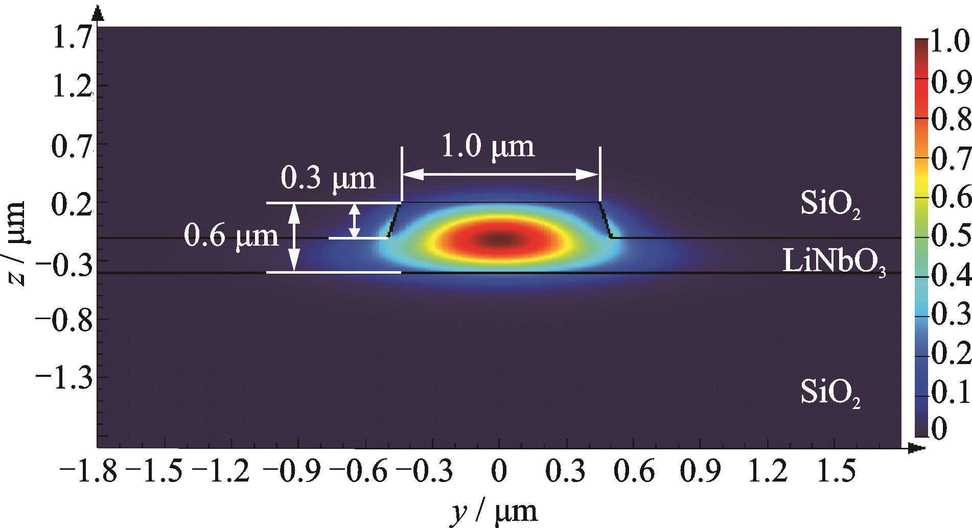
    Fig. 2. TE mode field diagram of arrayed waveguide
    The relationship between normalized output optical power and bending radius
    Fig. 3. The relationship between normalized output optical power and bending radius
    The relationship between normalized output optical power and waveguide spacing
    Fig. 4. The relationship between normalized output optical power and waveguide spacing
    LNOI arrayed waveguide grating
    Fig. 5. LNOI arrayed waveguide grating
    LNOI waveguide upper surface and end face before and after polishing
    Fig. 6. LNOI waveguide upper surface and end face before and after polishing
    Spectral response of LNOI arrayed waveguide grating
    Fig. 7. Spectral response of LNOI arrayed waveguide grating
    参数数值
    中心波长/nm1 550
    相邻通道间隔/GHz400(~3.2 nm)
    自由光谱范围/nm16.0
    阵列波导长度差/μm64.71
    罗兰圆直径/μm177
    阵列波导数31
    Table 1. Structure parameters of LNOI array waveguide grating
    Chenquan WANG, Fengjie ZHOU, Xiaowen GU, Jie TANG, Guang QIAN. Design and Fabrication of LNOI Arrayed Waveguide Grating[J]. Optoelectronic Technology, 2021, 41(4): 258
    Download Citation