• Opto-Electronic Advances
  • Vol. 6, Issue 3, 220101 (2023)
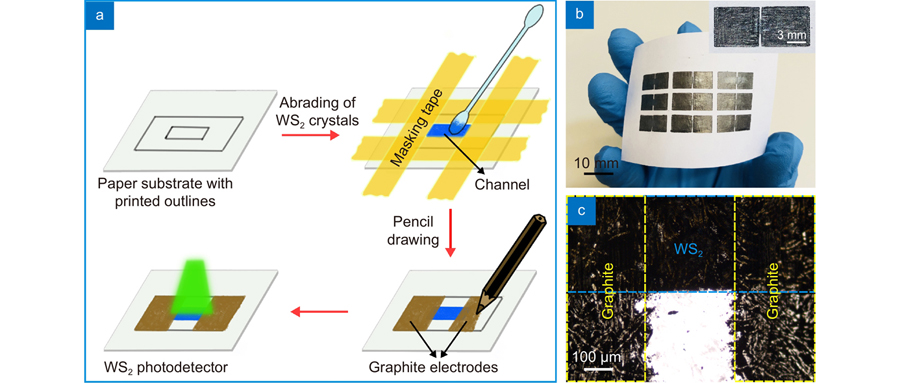
Wenliang Zhang1, Onur Çakıroğlu1, Abdullah Al-Enizi2, Ayman Nafady2..., Xuetao Gan3, Xiaohua Ma4, Sruthi Kuriakose1, Yong Xie1,4,* and Andres Castellanos-Gomez1,**|Show fewer author(s)
Author Affiliations
  • 1Materials Science Factory, Instituto de Ciencia de Materiales de Madrid (ICMM-CSIC), Madrid E-28049, Spain
  • 2Department of Chemistry, College of Science, King Saud University, Riyadh 11451, Saudi Arabia
  • 3Key Laboratory of Light Field Manipulation and Information Acquisition, Ministry of Industry and Information Technology, and Shaanxi Key Laboratory of Optical Information Technology, School of Physical Science and Technology, Northwestern Polytechnical University, Xi’an 710129, China
  • 4School of Advanced Materials and Nanotechnology, Xidian University, Xi’an 710071, China
  • show less
    DOI: 10.29026/oea.2023.220101 Cite this Article
    Wenliang Zhang, Onur Çakıroğlu, Abdullah Al-Enizi, Ayman Nafady, Xuetao Gan, Xiaohua Ma, Sruthi Kuriakose, Yong Xie, Andres Castellanos-Gomez. [J]. Opto-Electronic Advances, 2023, 6(3): 220101 Copy Citation Text show less
    (a) Schematic illustration of the fabrication process of paper-based WS2 photodetectors via abrading WS2 crystals and penciling graphite electrodes on paper substrates. (b) Photograph of the 3 × 3 WS2 photodetector array. Inset shows the magnified view of a WS2 photodetector. (c) Optical micrograph of a WS2 photodetector showing the WS2 channel and graphite electrode regions.
    Fig. 1. (a) Schematic illustration of the fabrication process of paper-based WS2 photodetectors via abrading WS2 crystals and penciling graphite electrodes on paper substrates. (b) Photograph of the 3 × 3 WS2 photodetector array. Inset shows the magnified view of a WS2 photodetector. (c) Optical micrograph of a WS2 photodetector showing the WS2 channel and graphite electrode regions.
    Comparison of the photoresponse performance of the paper-based WS2 photodetector (device A) tested in air and vacuum conditions under illumination. (a) Current vs. time across the device under a periodic ON/OFF switching of illumination with a power intensity of 35 mW cm−2. (b) Zoomed in on three consecutive ON/OFF cycles from (a). (c) Photocurrent vs. time for the WS2 device as the illumination is switched ON/OFF with increasing incident power intensity from 1.1 mW cm−2 to 35 mW cm−2. (d) Photocurrent as a function of the power intensity. Note: Measurements are carried out at a bias voltage of 10 V and with a selected wavelength of 617 nm. The channel length and width of the device A are ~300 μm and 2 mm, respectively.
    Fig. 2. Comparison of the photoresponse performance of the paper-based WS2 photodetector (device A) tested in air and vacuum conditions under illumination. (a) Current vs. time across the device under a periodic ON/OFF switching of illumination with a power intensity of 35 mW cm−2. (b) Zoomed in on three consecutive ON/OFF cycles from (a). (c) Photocurrent vs. time for the WS2 device as the illumination is switched ON/OFF with increasing incident power intensity from 1.1 mW cm−2 to 35 mW cm−2. (d) Photocurrent as a function of the power intensity. Note: Measurements are carried out at a bias voltage of 10 V and with a selected wavelength of 617 nm. The channel length and width of the device A are ~300 μm and 2 mm, respectively.
    Voltage-dependent photoresponse of the paper-based WS2 photodetector (device B) under the illumination of 617 nm. (a) Photocurrent as a function of time for the WS2 photodetector while the light is switched ON/OFF under various power intensities at a fixed bias voltage of 35 V. (b) The measured photocurrent and (c) corresponding responsivity as a function of power intensity collected at various bias voltages from 1 to 35 V. (d) The measured photocurrent and responsivity as a function of bias voltage at a fixed power intensity of 35 mW cm−2.
    Fig. 3. Voltage-dependent photoresponse of the paper-based WS2 photodetector (device B) under the illumination of 617 nm. (a) Photocurrent as a function of time for the WS2 photodetector while the light is switched ON/OFF under various power intensities at a fixed bias voltage of 35 V. (b) The measured photocurrent and (c) corresponding responsivity as a function of power intensity collected at various bias voltages from 1 to 35 V. (d) The measured photocurrent and responsivity as a function of bias voltage at a fixed power intensity of 35 mW cm−2.
    Spectral response of the paper-based WS2 photodetector (device B). (a) Photocurrent vs. time when the device is subjected to cycles of ON/OFF illumination with different wavelengths. (b) Spectrum response of the WS2 photodetector under various wavelengths of illumination in the range of 365 nm (ultraviolet) to 940 nm (near-infrared). Note: The device is measured at a fixed voltage of 10 V and an incident power intensity of 13 mW cm−2.
    Fig. 4. Spectral response of the paper-based WS2 photodetector (device B). (a) Photocurrent vs. time when the device is subjected to cycles of ON/OFF illumination with different wavelengths. (b) Spectrum response of the WS2 photodetector under various wavelengths of illumination in the range of 365 nm (ultraviolet) to 940 nm (near-infrared). Note: The device is measured at a fixed voltage of 10 V and an incident power intensity of 13 mW cm−2.
    Integration of the paper-based WS2 photodetector as detection element in an optical spectrometer. (a) Schematic diagram of the spectrometer system consist of a light source, a light-scattering optical element (reflective diffraction grating), and a detection element. (b) The measured power profiles using a commercial silicon photodiode and (c) photocurrent profiles using the paper-based WS2 photodetector (device C). Note: As light source we have used a supercontinuum laser with different spectral filters.
    Fig. 5. Integration of the paper-based WS2 photodetector as detection element in an optical spectrometer. (a) Schematic diagram of the spectrometer system consist of a light source, a light-scattering optical element (reflective diffraction grating), and a detection element. (b) The measured power profiles using a commercial silicon photodiode and (c) photocurrent profiles using the paper-based WS2 photodetector (device C). Note: As light source we have used a supercontinuum laser with different spectral filters.
    Material/DeviceSubstrateFabrication techniqueBias voltage(V)Power intensity(mW cm−2)Responsivity(mA W−1)Responsetime (s)Ref.
    WS2/GrapheneTechnical paper (PEL P60)Inkjet printing2.544.1−172.60.61~5ref.59
    Graphene(bottom)/WS2/Graphene(top)Technical paper(PEL P60)Inkjet printing17~1ref.39
    MoS2PaperRubbing process217.46−111.940.01~20−30ref.5
    ZnS-MoS2PaperHydrothermal19.10.0178511rref.58
    MoS2/WSe2PaperDrop cast551240.1r; 0.3fref.37
    WSe2/AgPhotocopy paperRubbing process10.37−0.900.07257.5ref.67
    WSe2 nanodotsFilter paperDip coating5117.780.68r; 1.01fref.56
    WSe2/GraphitePaperDrop cast156.660.8r; 1.4fref.41
    ZnO/GraphenePaperDirect writing3.96.278.76r; 18.13fref.68
    WS2 nanosheetsFilter membraneVacuum filtration559.094.0411.6r; 7.9fref.60
    Multilayer WS2QuartzCVD0.0925.3×10−3ref.61
    WS2Si waferDrop cast12140~2.50.03−0.07ref.69
    WS2Si waferMagnetron sputtering01541.1×10−6rref.65
    GOQDs-WS2Si waferMechanical exfoliation512.50.0326r; 0.0275fref.66
    WS2PIMagnetron sputtering and electron beam irradiation103.91.660.48−0.86r;0.70−0.88fref.64
    Monolayer WS2PICVD100.0750.12rref.62
    WS2PENCVD68.3×105~5×10⁻³~0.08ref.63
    WS2/GraphitePETMechanical abrasion2552411.8r; 20.5fref.31
    WS2/GraphitePaperAll-dry abrasion1−3535.031.2 at 1 V;6.4 at 5 V;14.3 at 10 V;268.7 at 35 V7.31r; 6.58fThis work
    WS2/AuPaperAll-dry abrasion535.03193.94.12r; 4.14fThis work
    Table 1. Comparison of typical device characteristics of the present WS2 in this work and other TMDCs-based and paper-supported photodetection devices. Response time values highlighted with r or f represent the rise time and fall time values, respectively.
    Wenliang Zhang, Onur Çakıroğlu, Abdullah Al-Enizi, Ayman Nafady, Xuetao Gan, Xiaohua Ma, Sruthi Kuriakose, Yong Xie, Andres Castellanos-Gomez. [J]. Opto-Electronic Advances, 2023, 6(3): 220101
    Download Citation