[1] O Uteza, Re B Bussi, F Canova, et al. Laser-induced damage threshold of sapphire in nanosecond, picosecond and femtosecond regimes. Applied Surface Science, 254, 799-803(2007).
[2] X Xie, C Zhou, X Wei, et al. Laser machining of transparent brittle materials: from machining strategies to applications. Opto-Electronic Advances, 2, 180017(2019).
[3] M Liu, Y Hu, X Sun, et al. Chemical etching mechanism and properties of microstructures in sapphire modified by femtosecond laser. Applied Physics A, 123, 99(2016).
[4] Jiaqun Li, Jianfeng Yan, Xi Li, . Research advancement on ultrafast laser microprocessing of transparent dielectrics. Chinese Journal of Lasers, 48, 0202019(2021).
[5] I Miyamoto, Y Okamoto, A Hansen, et al. High speed, high strength microwelding of Si/Glass using ps-laser pulses. Opt Express, 23, 3427-3439(2015).
[6] S A Lee, J Y Hwang, J P Kim, et al. Dielectric characterization of transparent epitaxial Ga2O3 thin film on n-GaN∕Al2O3 prepared by pulsed laser deposition. Applied Physics Letters, 89, 182906(2006).
[7] Z Li, X Wang, J Wang, et al. Stealth dicing of sapphire sheets with low surface roughness, zero kerf width, debris/crack-free and zero taper using a femtosecond bessel beam. Optics & Laser Technology, 135, 106713(2021).
[8] K Liao, W Wang, X Mei, et al. High quality full ablation cutting and stealth dicing of silica glass using picosecond laser bessel beam with burst mode. Ceramics International, 48, 9805-9816(2022).
[9] Y Lu, Y Li, X Xie, et al. Research advances of femtosecond laser-induced nanogratings for transparent materials. Front Chem, 10, 1082651(2022).
[10] S Han, H Yu, C He, et al. Laser slicing of 4H-SiC wafers based on picosecond laser-induced micro-explosion via multiphoton processes. Optics & Laser Technology, 154, 108323(2022).
[11] H Morisaki, F W Ping, H Ono, et al. Above-band-gap photoluminescence from Si fine particles with oxide shell. Journal of Applied Physics, 70, 1869-1870(1991).
[12] A F Mohammed, Q A Al-Jarwany, A J Clarke, et al. Ablation threshold measurements and surface modifications of 193 nm laser irradiated 4H-SiC. Chemical Physics Letters, 713, 194-202(2018).
[13] Rtner R Weing, P J Wellmann, M Bickermann, et al. Determination of charge carrier concentration in n- and p-doped SiC based on optical absorption measurements. Applied Physics Letters, 80, 70-72(2002).
[14] B Yang, H Wang, S Peng, et al. Precision layered stealth dicing of SiC wafers by ultrafast lasers. Micromachines, 13, 1011(2022).
[15] D Andiwijayakusuma, M Saito, A Purqon. Density functional theory study: Electronic structures of RE: GaN in wurtzite Gα15RE1N16. Journal of Physics: Conference Series, 739, 012027(2016).
[16] S T Yang, M J Matthews, S Elhadj, et al. Thermal transport in CO2 laser irradiated fused silica: In situ measurements and analysis. Journal of Applied Physics, 106, 103106(2009).
[17] Heisterkamp A, Leyder S, Herman P R, et al. On the wavelength dependence of femtosecond laser interactions inside b gap solids [C]Frontiers in Ultrafast Optics: Biomedical, Scientific, Industrial Applications XIII, SPIE LASE, 2013, 8611: 861113.
[18] G A Bufetova, V V Kashin, S Y Rusanov, et al. Determination of sapphire crystal melt refracttive index in visible range. Journal of Crystal Growth, 575, 126355(2021).
[19] M V Kondrin, Y B Lebed, V V Brazhkin. Intrinsic planar defects in diamond and the upper limit on its melting temperature. Diamond and Related Materials, 110, 108114(2020).
[20] Z Cao, D Aslam. Fabrication technology for single-material MEMS using polycrystalline diamond. Diamond and Related Materials, 19, 1263-1272(2010).
[21] D A Boysen, S M Haile, H Liu, et al. Conductivity of potassium and rubidium dihydrogen phosphates at high temperature and pressure. Chemistry of Materials, 16, 693-697(2004).
[22] Bihui Hou, Yali Wang, Xinan Chang, . THz-ultraviolet spectra of KDP crystal. Spectroscopy and Spectral Analysis, 30, 2881-2884(2010).
[23] A Kumar, R Kumar, N Verma, et al. Effect of the band gap and the defect states present within band gap on the non-linear optical absorption behaviour of yttrium aluminium iron garnets. Optical Materials, 108, 110163(2020).
[24] Sheng Feng, Zhitao Shan, Ruikun Pan, . Thermo-physical property of YAG melt measured by aerodynamic levitation technique. Journal of Inorganic Materials, 33, 1297-1302(2018).
[25] A Pavlik, S V Ushakov, A Navrotsky, et al. Structure and thermal expansion of Lu2O3 and Yb2O3 up to the melting points. Journal of Nuclear Materials, 495, 385-391(2017).
[26] G Seguini, E Bonera, S Spiga, et al. Energy-band diagram of metal/Lu2O3/silicon structures. Applied Physics Letters, 85, 5316-5318(2004).
[27] W C Wang, M Badylevich, V V Afanas’ev, et al. Band alignment and electron traps in Y2O3 layers on (100)Si. Applied Physics Letters, 95, 132903(2009).
[28] Meiling Luan, Jiaxin Zheng, Xiangchao Sun, . Liquid-assisted laser fabrication of hard materials and applications. Opto-Electronic Engineering, 50, 61-78(2023).
[29] R Srinivasasn, E Sutcliffe, B Braren. Ablation and etching of polymethylmethacrylate by very short (160 fs) ultraviolet (308 nm) laser pulses. Applied Physics Letters, 51, 1285-1287(1987).
[30] C W Cheng, X Z Tsai, J S Chen. Micromachining of stainless steel with controllable ablation depth using femtosecond laser pulses. The International Journal of Advanced Manufacturing Technology, 85, 1947-1954(2016).
[31] S Hunsche, K Leo, H Kurz, et al. Exciton absorption saturation by phase-space filling: Influence of carrier temperature and density. Phys Rev B Condens Matter, 49, 16565-16568(1994).
[32] Z Fang, J Chen, X Jiang, et al. Repair of fused silica damage using selective femtosecond laser-induced etching. Crystals, 13, 309(2023).
[33] F V Grigogrev, V B Sulimov, A V Tikhonravov. Laser-induced thermal stresses in dense and porous silicon dioxide films. Coatings, 11, 394(2021).
[34] P Polynkin. Intense femtosecond shaped laser beams for writing extended structures inside transparent dielectrics. Applied Physics A, 114, 143-149(2013).
[35] A M Zheltikov. Ultrafast optical switching of an ionized medium by interfering ultrashort laser pulses. JETP Letters, 90, 90-95(2009).
[36] K Hu, Z Guo, T Cao, et al. Study on the polarization dependence of nonlinear absorption of ultrafast laser pulses in bulk fused silica. Opt Express, 30, 8949-8958(2022).
[37] S Wu, D Wu, J Xu, et al. Characterization and mechanism of glass microwelding by double-pulse ultrafast laser irradiation. Optics Express, 20, 28893-28905(2012).
[38] A Bogatskaya, Y Gulina, N Smirnov, et al. An experimental study of multiphoton ionization in fused silica at IR and visible wavelengths. Photonics, 10, 515(2023).
[39] K M Koz, N F Troj, P Mal. Hot-carrier transport in diamond controlled by femtosecond laser pulses. New Journal of Physics, 17, 053027(2015).
[40] M R Marks, K Y Cheong, Z Hassan. A review of laser ablation and dicing of Si wafers. Precision Engineering, 73, 377-408(2022).
[41] C W Ponader, J F Schroeder, A M Sterltsov. Origin of the refractive-index increase in laser-written waveguides in glasses. Journal of Applied Physics, 103, 063516(2008).
[42] K Miura, J Qiu, H Inouye, et al. Photowritten optical waveguides in various glasses with ultrashort pulse laser. Applied Physics Letters, 71, 3329-3331(1997).
[43] O M Efimov, L B Glebov, K A Richardson, et al. Waveguide writing in chalcogenide glasses by a train of femtosecond laser pulses. Optical Materials, 17, 379-386(2001).
[44] F M Bain, W F Silva, A Lagatskya, et al. Microspectroscopy of ultrafast laser inscribed channel waveguides in Yb: tungstate crystals. Applied Physics Letters, 98, 141108(2011).
[45] L Sudrie, M Franco, B Prade, et al. Writing of permanent birefringent microlayers in bulk fused silica with femtosecond laser pulses. Optics Communications, 171, 279-284(1999).
[46] F Liang, R Vallee, S L Chin. Mechanism of nanograting formation on the surface of fused silica. Opt Express, 20, 4389-4396(2012).
[47] R Taylor, C Hnatovsky, E Simove. Applications of femtosecond laser induced self-organized planar nanocracks inside fused silica glass. Laser & Photonics Review, 2, 26-46(2008).
[48] S Richter, M Heinrich, Ring S D, et al. Nanogratings in fused silica: Formation, control, and applications. Journal of Laser Applications, 24, 042008(2012).
[49] W Cheng, Z Wang, X Liu, et al. Microexplosions in bulk sapphire driven by simultaneously spatially and temporally focused femtosecond laser beams. Opt Lett, 48, 751-754(2023).
[50] Nana Peng, Yanyan Huo, Kan Zhou, . The development of femtosecond laser-induced periodic nanostructures and their optical properties. Acta Physica Sinica, 62, 9-16(2013).
[51] Yiming Lu, Bingrong Gao, Xueqing Liu, . Fabrication of high temperature resistant geometric phase element inside sapphire by femtosecond laser (Invited). Acta Photonica Sinica, 50, 0650107(2021).
[52] Y Shimotsuma, P G Kazansky, J Qiu, et al. Self-organized nanogratings in glass irradiated by ultrashort light pulses. Phys Rev Lett, 91, 247405(2003).
[53] S Juodkazis, K Nishimura, S Tanaka, et al. Laser-induced microexplosion confined in the bulk of a sapphire crystal: Evidence of multimegabar pressures. Physical Review Letters, 96, 166101(2006).
[54] Y Huang, X Wu, H Liu, et al. Fabrication of through-wafer 3D microfluidics in silicon carbide using femtosecond laser. Journal of Micromechanics and Microengineering, 27, 065005(2017).
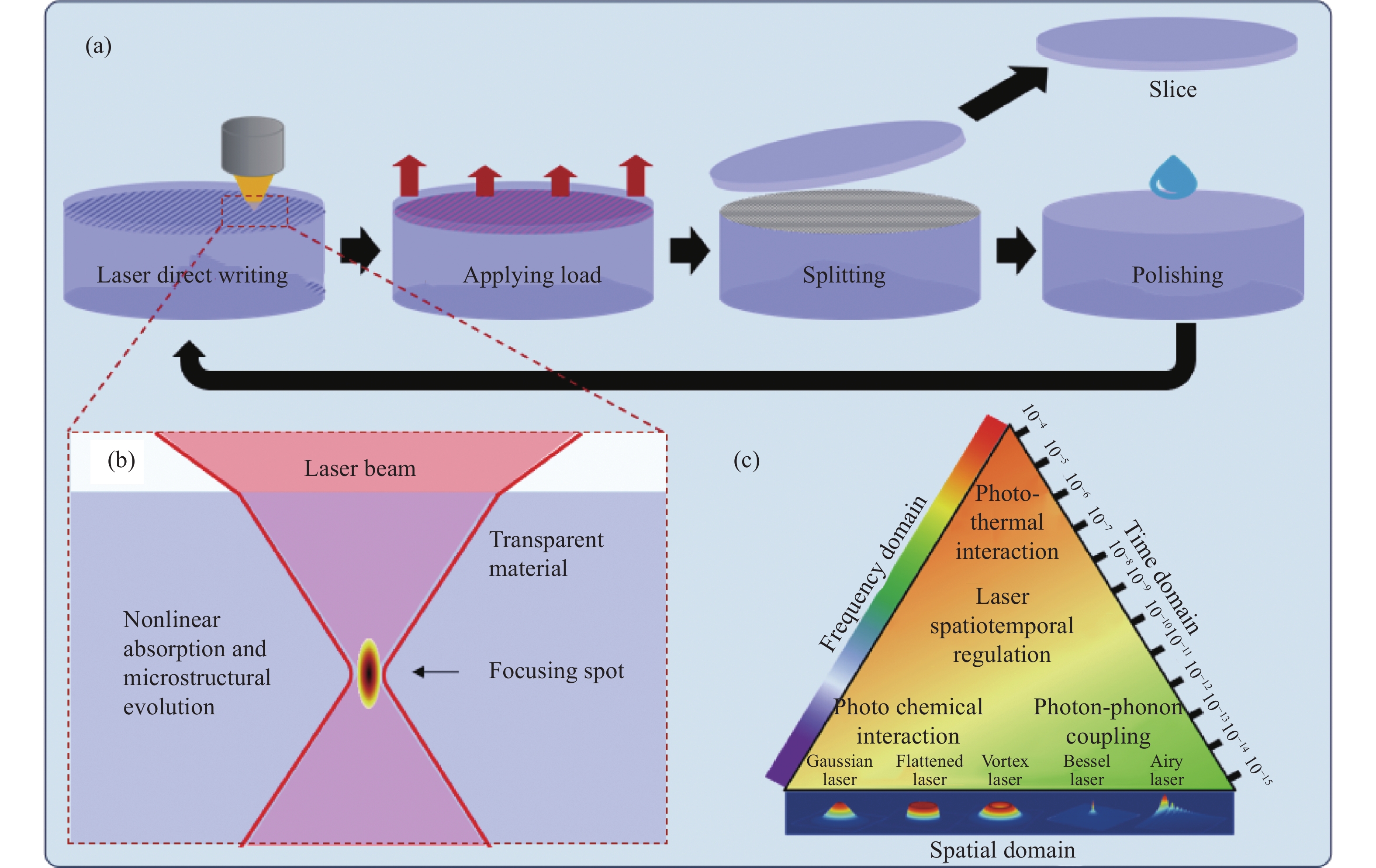
[55] J Wang, F Fang, H An, et al. Laser machining fundamentals: micro, nano, atomic and close-to-atomic scales. International Journal of Extreme Manufacturing, 5, 012005(2023).
[56] Z Zhai, W Wang, J Zhao, et al. Influence of surface morphology on processing of C/SiC composites via femtosecond laser. Composites Part A: Applied Science and Manufacturing, 102, 117-125(2017).
[57] Ohmura E. Temperature Rise of Silicon due to Absption of Permeable Pulse Laser [M]Heat TransferEngineering Applications. London: IntechOpen, 2011.
[58] E Paoagiakoumou, E Ronzitti, V Emiliani. Scanless two-photon excitation with temporal focusing. Nat Methods, 17, 571-581(2020).
[59] P S Salter, M J Booth. Adaptive optics in laser processing. Light Sci Appl, 8, 110(2019).
[60] P S Salter, M Baum, I Alexeev, et al. Exploring the depth range for three-dimensional laser machining with aberration correction. Opt Express, 22, 17644-17656(2014).
[61] E Kim, Y Shimotsuma, M Sakakura, et al. 4H-SiC wafer slicing by using femtosecond laser double-pulses. Optical Materials Express, 7, 2450(2017).
[62] X Jia, Y Chen, L Liu, et al. Combined pulse laser: Reliable tool for high-quality, high-efficiency material processing. Optics & Laser Technology, 153, 108209(2022).
[63] J Hernandez-rueda, J Siegel, D Puerto, et al. Ad-hoc design of temporally shaped fs laser pulses based on plasma dynamics for deep ablation in fused silica. Applied Physics A, 112, 185-189(2012).
[64] A Rosenfeld, M Rohloff, Hm S H, et al. Formation of laser-induced periodic surface structures on fused silica upon multiple parallel polarized double-femtosecond-laser-pulse irradiation sequences. Applied Surface Science, 258, 9233-9236(2012).
[65] Wenfeng Liu, Mingying Sun, Yiqun Shi, . Picosecond laser ablation of glass surface by dual-pulse temporal. Chinese Journal of Lasers, 50, 1202201(2023).
[66] Hongqing Wang, Jisen Wen, Zhenyao Yang, . High-speed parallel two-photon laser direct writing lithography system. Chinese Journal of Lasers, 49, 2202009(2022).
[67] X W Cao, Y M Lu, H Fan, et al. Wet-etching-assisted femtosecond laser holographic processing of a sapphire concave microlens array. Appl Opt, 57, 9604-9608(2018).
[68] E K Sanchez, S Ha, J Grim, et al. Assessment of polishing-related surface damage in silicon carbide. Journal of the Electrochemical Society, 149, G131(2002).
[69] J R Grim, M Benamara, M Skowronski, et al. Transmission electron microscopy analysis of mechanical polishing-related damage in silicon carbide wafers. Semiconductor Science and Technology, 21, 1709-1713(2006).
[70] Shi Erwei. The Growth Defects of Silicon Carbide Crystal [M]. Beijing: Science Press, 2012. (in Chinese)
[71] M Swoboda, C Beyer, R Rieske, et al. Laser assisted SiC wafering using cold split. Materials Science Forum, 897, 403-406(2017).
[72] Kling R, Washio K, Klotzbach U, et al. New laser slicing technology named KABRA process enables high speed high efficiency SiC slicing [Z]. Laserbased Micro Nanoprocessing XII, 2018.
[73] H Wang, Q Chen, Y Yao, et al. Influence of surface preprocessing on 4H-SiC wafer slicing by using ultrafast laser. Crystals, 13, 15(2022).
[74] Y Zhang, X Xie, Y Huang, et al. Internal modified structure of silicon carbide prepared by ultrafast laser for wafer slicing. Ceramics International, 49, 5249-5260(2023).
[75] W Geng, Q Shao, Y Pei, et al. Slicing of 4H-SiC wafers combining ultrafast laser irradiation and bandgap-selective photo-electrochemical exfoliation. Advanced Materials Interfaces, 10, 202300200(2023).
[77] Delphi Laser. Laser processing equipment f silicon carbide wafers [EBOL]. (20230710) [20231019]. http:www.delphilaser.comcontent319.
[78] Westlake Instruments. SiC substrate laser peeling equipment [EBOL]. (20230524) [20231019]. http:www.westlakeinst.comproducts61.html.
[79] Disco. Development of a KABRA® Process Optimized f the Production of GaN Wafers [EBOL]. (20211001) [20231019]. https:www.disco.co.jpegnewscpkabra_gan.html.
[80] V Voronenkov, N Bochkareva, R Gorbunov, et al. Laser slicing: A thin film lift-off method for GaN-on-GaN technology. Results in Physics, 13, 102233(2019).
[81] F Kaule, M Swoboda, C Beyer, et al. Laser-assisted spalling of large-area semiconductor and solid state substrates. MRS Communications, 8, 127-131(2018).
[82] F Dross, J Robbelein, B Vandevelde, et al. Stress-induced large-area lift-off of crystalline Si films. Applied Physics A, 89, 149-152(2007).
[83] H Hirai, H Hidai, S Matsusaka, et al. Diamond slicing using ultrashort laser-induced graphitization and additional nanosecond laser illumination. Diamond and Related Materials, 96, 126-133(2019).
[84] F Kiel, N M Bulgakova, A Ostendorf, et al. Selective delamination upon femtosecond laser ablation of ceramic surfaces. Physical Review Applied, 11, 024038(2019).