
Yingkang YANG, Yiqing SHAO, Bailiang LI, Zhiwei LÜ, Lulu WANG, Liangjun WANG, Xun CAO, Yuning WU, Rong HUANG, Chang YANG. Enhanced Band-edge Luminescence of CuI Thin Film by Cl-doping [J]. Journal of Inorganic Materials, 2023, 38(6): 687
- Journal of Inorganic Materials
- Vol. 38, Issue 6, 687 (2023)
Abstract
γ-CuI is a p-type transparent semiconductor material with a wide and direct bandgap of 3.05 eV at room temperature. Its high exciton binding energy (58 meV), high hole mobility (>40 cm2·V-1·s-1 in bulk)[1-2], large Seebeck coefficient and low thermal conductivity made it promising for optoelectronic and thermoelectric applications[1⇓⇓⇓⇓⇓⇓-8]. It has been integrated with other semiconductors such as GaN[9], ZnO[10], and β-Ga2O3[11] for fabrication of heterostructure devices. In addition, CuI is suitable for large-scale fabrication because of its low cost and mild synthesis conditions.
In recent years, excellent luminescence property of CuI have attracted wide interest. The PL peak of CuI film reported by Ahn, et al.[9] was one order of magnitude higher than that of commercial undoped GaN film at room temperature, and a hybrid n-GaN/p-CuI blue LED was developed. The luminescence of CuI at the room temperature is composed of the near-band-edge (NBE) emission and deep-level (DL) emission. The NBE emission consists of a sharp peak at 410 nm originated from the recombination of free excition and a broad band at 420-430 nm related to its intrinsic defects such as the copper vacancies and excess I[12]. The DL emission exhibits a broad band at 680-720 nm, which is originated from the I vacancies[13-14]. Yu, et al.[15] investigated the effect of growth temperature on luminescence performance of sputtered CuI thin film, and optimized the optical performance at 300 ℃. Chen, et al.[16] reported efficient photoluminescence ink prepared using Cu-I cluster-based hybrid materials for biological imaging. However, it is still a challenge to promote the NBE emission (especially the band-edge emission) and meanwhile suppress the DL emission for potential applications.
Halogen doping is one of the most important strategy to tailor the luminescence of CuI. The Ⅰ-VII copper halides including CuCl, CuBr and CuI are all p-type wide bandgap semiconductors with high exciton binding energies of 190, 108, and 58 meV[17], respectively, which are believed to show excellent luminescence property. The luminance of polycrystalline CuCl films on Si substrate is 23 orders of magnitude higher than that of undoped single crystal GaN at room temperature[18]. When Cl or Br substitute I site in the CuI lattice, the difference in the p-orbital energy level of halogen elements can significantly affect the electronic structure and defect energy level position of CuI[19]. Li, et al.[13] found that Cl doping can enhance the NBE emission and suppress the DL emission of CuI effectively with an optimum concentration of 10% (in mol). However, most of researches focused on the photoluminescence of CuI single crystal and powder samples synthesized at relatively high temperature. In this work, Cl-doped CuI thin films were investigated in detail by scanning electron microscope (SEM) and cathodoluminescence spectroscope (CL). The band-edge emission at 410 nm and the DL emission within 680-720 nm from the areas with different doping levels were compared. The mechanism of the enhanced band-edge emission by Cl doping was revealed by the first principles calculations.
1 Experimental
1.1 Preparation of the film
The Cl-doped CuI film was prepared by gas-phase reaction method. The copper film was prepared by magnetron sputtering with Ar gas pressure of 2 Pa. A copper metal target and a quartz substrate were used for sputtering with a DC power of 30 W for 5 min. The thickness of obtained Cu thin film was about 70 nm. The obtained Cu film sample was placed together with 10 g iodine particles (purity of 99.9%) and trace CuCl solution (CuCl was dissolved in ethanol at 1% (in mass)) in a quartz glass bottle with a height of 5 cm and a diameter of 3 cm, which was sealed and kept at 80 ℃ on a hot plate for 20 min for iodization and Cl doping at the same time. The obtained Cl-doped CuI thin film exhibited a thickness of about 220 nm.
1.2 Characterization of the thin film
The morphology of Cl-doped CuI thin films was observed by a scanning electron microscope (Zeiss Gemini SEM450) equipped with an X-ray energy dispersive spectrometer (EDS: Oxford UltimMax EXTREME) for the chemical analyses and a CL spectrometer (Gatan Monarc Pro) for the CL analyses. The accelerating voltages were set at 2 kV for imaging and 5 kV for analyses. The grating 300 lines/mm and the resolution of 0.32 nm were used for the CL analyses at room temperature.
1.3 Computational methods
The first-principles calculations were performed using density functional theory (DFT)[20-21] as implemented in the Quantum-Espresso package[22]. The structural optimization was done using Perdew-Burke-Eznerhof (PBE)[23] exchange-correlation functional, and the defect properties including formation energies and transition levels were based on Hybrid HSE06[24] functional. The energy cutoff for the plane-wave basis was selected as 450 eV, and a 216-atom supercell was employed for defect calculations. For type of each defect, the defect is constructed in this supercell. For example, ClI is simulated by substituting one out of 108 I atoms by a Cl atom.
The formation enthalpy $\Delta {{H}_{f}}(\alpha,q)$ of a defect $\alpha $ in the charge state q using the supercell model can be calculated using[25⇓⇓-28]
where $E(\alpha,q)$ is the total energy of the supercell with a defect $\alpha $ and charge state $q$, and $E(\text{host})$ is the total energy of the host perfect crystal. ${{n}_{i}}$ is the number of the atoms of element I removed from (${{n}_{i}}$ is negative) or added to (${{n}_{i}}$ is positive) the supercell when forming the defect. ${{E}_{i}}$ is the energy per atom of element I in its stable elemental phase, and ${{\mu }_{i}}\text{ }\!\!~\!\!\text{ }$ is the chemical potential of element I. ${{E}_{\text{corr}}}$, which comes from the Coulomb interaction among the repeating charged defects, was treated using scheme of Lany and Zunger[26]. The Fermi level ${{E}_{\text{F}}}$ can vary from 0 to bandgap, and ${{\varepsilon }_{\text{VBM}}}$ is the valence band maximum (VBM) of the host system.
2 Results and discussion
2.1 Surface morphology
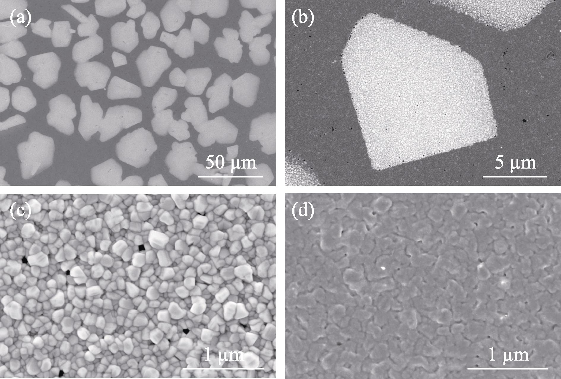
Fig. 1(a) shows a typical low magnification surface morphology of Cl-doped CuI thin film. Many irregular bright regions with the size of tens of micrometers can be seen in the dark background. The interface between the bright region and the dark region is very sharp and clear, as shown in Fig. 1(b). At high magnification (Fig. 1(c)), the bright regions exhibit the granular morphology with the grain size of ~100 nm, which is similar to the grain morphology of polycrystalline CuI films reported in the literature[1]. However, as shown in Fig. 1(d), the grains observed in the dark region are densely packed and connected, resulting in blurry grain boundaries and a relatively flat surface.
![]()
Figure 1.Typical SEM images of the Cl-doped CuI thin film(a) Low magnification; (b) High magnification; (c) High magnification image of the bright region; (d) High magnification image of the dark region
In order to know the difference between the regions with different contrast, EDS analyses were employed to obtain the chemical composition. Fig. 2(a) shows the SEM image of the EDS mapping area. Fig. 2(c) shows the corresponding Cu, I, Cl and Si elemental mappings. It can be seen that the contrast of Cu and I mappings are uniform. No obvious differences between the bright and dark regions can be discerned. However, relatively bright contrast can be seen in the dark regions of the Cl map. To confirm the Cl-rich in the dark region, two EDS spectra from the bright region (red) and the dark region (blue) were compared in Fig. 2(b) with the normalization of the Cu-L peak. An apparent Cl-K peak appears in the dark region. The quantifications of the EDS spectra reveal that the Cl concentration in the dark region is 2.69% (in mol) whereas the bright region keeps pure CuI. The lower anion/cation ratio in the dark region compared with the bright region indicates that the CuI sample is closer to the stoichiometry after Cl-doping.
![]()
Figure 2.EDS analyses of the Cl-doped CuI thin film(a) SEM image of the mapping area; (b) Typical EDS spectra obtained from the bright region and the dark region; (c) EDS mappings of Cu, I, Cl and Si
In the synthesis of CuI thin film by gas-phase reaction, a small amount of Cl dopant reached the sample surface, occupying the I sites on the grain surface, and then diffused into the film. However, the distribution of Cl was not uniform due to the uncontrollable vapor flow. Also, the substrate temperature of ~80 ℃ was not high enough for sufficient Cl migration to reach the lowest free energy positions on the rough CuI surface, leading to surface phase segregations towards bright and dark regions. Such distinct two regions on the same sample were helpful for identifying the effects of Cl doping on CuI. Apparently, the Cl-doped dark region presented a more dense and flat morphology compared with the undoped bright region. Since Cl has a higher electron affinity than I and CuCl forms stronger bonding than CuI, it is likely that Cl can compensate the iodine-related defects on the CuI surface and thus improve the surface morphology. At the same time, replacing I with Cl leads to fewer copper vacancy defects, which should be the reason of the lowered anion/cation ratio.
![]()
Figure 3.CL analyses of the Cl-doped CuI thin film(a) SEM image; (b) Panchromatic CL image; (c) Typical CL spectra acquired from the bright region and the dark region
2.2 Luminescence property
Interestingly, the panchromatic CL images exhibited reversed contrast of SEM images, as shown in Fig. 3(a, b). The dark regions in the SEM image display brighter contrast in the CL image. It indicates that the emission intensity of the Cl-doped CuI regions is much stronger than the pure CuI regions. Fig. 3(c) shows typical CL spectra from the Cl-doped dark region (blue) and the bright pure CuI region (red) with exactly the same experimental conditions. A very sharp peak at 410 nm which originates from the band-edge emission and a broad DL emission at around 720 nm which might be caused by VI-related defects are observed in both spectra. However, the intensity of the 410 nm peak from the Cl-doped CuI is ~2.5 times of that from the pure CuI. Furthermore, the intensity ratio of the peaks at 410 and 720 nm increases from 13.4 to 38.5 after Cl doping, suggesting greatly enhanced band-edge emission and suppressed DL emission.
In addition, the band-edge emission at 410 nm doesn’t shift with the Cl-doping and no defects related NBE emission around 420 nm are detected in the present study, as shown in the inset of Fig. 3(c). It indicates negligible luminescence contributions from shallow energy level defects, which were abundant in the powder CuI samples synthesized at high temperature[14]. The full width at half maximum (FWHM) value of the band-edge emission peak is as small as 7 nm, better than many traditional LEDs[29-30], indicating an excellent monochromaticity of the Cl-doped CuI thin film. About 2.69% (in atom) Cl doping doubled the band-edge emission luminescence intensity of CuI, which might be related to the higher exciton binding energy of CuCl compared to CuI. The Cl dopant compensated the VI-related defects and the iodization of Cu film at low temperature (80 ℃) eliminated the formation of the VCu-related defects, resulting in strongly suppressed non-radiative recombination, the defects related NBE emission and DL emission. Consequently, an enhanced band-edge luminescence was obtained in Cl-doped CuI thin films.
To further understand the effects of Cl doping on the crystal defects in CuI thin films, the formation energies of various defects including the ClI substitution were calculated with the conditions of Cu-rich and I-rich by the first principles calculations. The results are shown in Fig. 4. It can be seen that the defect ClI is not ionized and maintains neutral for the whole range of bandgap, indicating that ClI does not introduce defect energy levels into the band gap. On the other hand, the formation energy of ClI substitution defects is only 0.10 eV under Cu-rich conditions and 0.58 eV under I-rich conditions (purple lines in Fig. 4). They are lower than most of the intrinsic defects in CuI, especially the defects such as VI that introduce deep levels into the band gap[31]. This means that the Cl dopant is easy to fill in I vacancy or replace I to form ClI, which effectively inhibits the generation of deep energy level defects such as VI. It reduces the probability of non-radiative transitions in excitons in Cl-doped CuI regions, leading to stronger luminescence intensity than that of the undoped CuI regions.
![]()
Figure 4.Calculated formation energies of ClI and the most intrinsic defects in CuI as functions of the Fermi level(a) Cu-rich condition; (b) I-rich condition
3 Conclusions
In summary, the Cl-doped CuI thin films made by the gas-phase reaction method consist of bright region (pure CuI) and dark region (Cl-doped CuI) in SEM image. The CL intensity of the 410 nm sharp peak originated from the band-edge emission in the Cl-doped region is more than two times of that in the undoped region, revealing greatly enhancement of the band-edge emission and effective suppression of the DL emission. The first principles calculations found that the ClI defect has a shallow forming energy. Thus, Cl doping might inhibit the defects in the VI iso-deep energy level effectively, thereby reducing the probability of non-radiative transitions in excitons. Our findings pave the way for the future development of high-performance CuI-based optoelectronic devices such as LEDs and scintillators by halogen doping.


Set citation alerts for the article
Please enter your email address

© Copyright 2018-2021 | Chinese Laser Press. All Rights Reserved 沪ICP备15018463号-20