Chaoyue Yan, Shengzhi Sun, Xiaofeng Liu, Jianrong Qiu. Research Progress on Preparation of Three-Dimensional Micro-Nano Connected Structures in Transparent Materials by Femtosecond Laser Material Reduction Method[J]. Laser & Optoelectronics Progress, 2023, 60(21): 2100001
Search by keywords or author
- Laser & Optoelectronics Progress
- Vol. 60, Issue 21, 2100001 (2023)
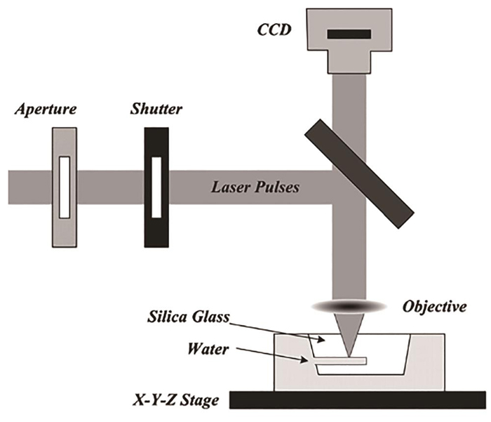
![Schematic diagram of liquid assisted femtosecond laser ablation[19]](/richHtml/lop/2023/60/21/2100001/img_01.jpg)
Fig. 1. Schematic diagram of liquid assisted femtosecond laser ablation[19]
![Microfluidic device diagram. (a) Fabricated microfluidic device at 500 µm below the surface of silica glass; (b) microfluidic device after heat treatment; (c) (d) micro-pools before heat treatment; (e) (f) micro-pools after heat treatment[20]](/richHtml/lop/2023/60/21/2100001/img_02.jpg)
Fig. 2. Microfluidic device diagram. (a) Fabricated microfluidic device at 500 µm below the surface of silica glass; (b) microfluidic device after heat treatment; (c) (d) micro-pools before heat treatment; (e) (f) micro-pools after heat treatment[20]
Fig. 3. Schematic diagram of processing flow. (a) Femtosecond laser direct writing creates 3D patterns in Foturan glass; (b) in the post-annealing step, the sample is heated in a programmable furnace; (c) diluted HF acid etches the sample[24]
Fig. 4. Examples of etched cones (top-view microscope pictures), obtained from tracks irradiated with orthogonal polarization at two different inscription pulse-energies (Ep = 2.2 µJ and Ep = 8.6 µJ), vt = 1 mm/s, and 25 kHz repetition-rate. Etching was performed in HF solution for 10 min or in KOH for 6 h (scale: 50 μm)[29]
Fig. 5. Etching rate of conventional pulses and double pulses as a function of the laser scanning speed at energy of (a) 0.5 μJ, (b) 1.5 μJ, and (c) 2 μJ; (d) relation curve between optimal laser scanning speed and irradiation energy[30]
Fig. 6. Schematic diagram of femtosecond laser dual pulse optical processing. (a) Experimental setup of the femtosecond laser microchannels drilling using single-pulse Bessel beams; (b) microscopic images of microchannels drilled in PMMA at pulse energy of 20 μJ by single-pulse Bessel beams; (c) SEM images of the microchannel entrance morphology; (d) enlargement of the region in Fig. (b); (e)‒(g) corresponding results by Gaussian beams; (h) microscopic image of microchannels fabricated at different focusing depths with steps of ∆z = 30 μm[31]
Fig. 7. Schematic diagram of microchannel. (a) Femtosecond laser generation schematics of three-dimensional microchannels inside bulk polymers; (b) oblique views on four non-discontinuous horizontal curved channel structures demonstrate the complete three-dimensional capabilities of the studied process[38]
Fig. 8. Device diagram. (a) Measurement setup; (b) fabrication setup[42]
Fig. 9. Schematic illustration of the setup for femtosecond laser generation of 3D microchannels inside bulk polymer[43]
Fig. 10. Images of several sections of the FLMP fabricated 3D multi-depth reservoir micromodel. (a) Red line illustrates the line profile scan path which goes through three pore spaces and two hexagonal pore bodies for each reservoir; (b) a zoom-in section of reservoir 3 where the image was focused at the etched surface; (c)‒(e) inlet portions of reservoirs 1, 2, and 3, respectively(scale: 250 µm)[43]
Fig. 11. STR of template generated by direct laser writing. (a) Polymer DNA double helix (scale: 500 µm); (b) reverse structure in fused silica glass (scale: 400 µm) with a minimum channel size of 20 µm; (c) spiral wound (scale: 900 µm); (d) staggered microfluidic spiral channels produced in fused silica glass, with a channel width of 74 µm and full of dyes (see illustration, scale: 140 µm); (e) polymer microstructure of out of plane mixer structure (scale: 600 µm); (f) fused silica glass microfluidic mixer structure with channel width of 74 µm (scale: 280 µm)[46]
Fig. 12. 3D microfluidic network production process. (a) 3D hand model; (b) schematic diagram of embedded microchannel pattern for ultrashort-pulse laser-assisted chemical etching; (c) before and (d) after CO2 laser sealing; (e) based on a combination of 3D glass subtractive printing and hybrid laser microfabrication 3D microfluidics demonstration of the hand; (f) close-up image of a part of the hand [as indicated by the white arrow in Fig.(e)][49]
Fig. 13. Schematic of FLAE-TPP for “ship-in-a-bottle” polymer integration. (a) Laser irradiation of Foturan; (b) microchannel developed after etching; (c) TPP of SU-8 photoresist inside microchannel; (d) 3D polymeric patterns (as indicated by the black arrow) developed inside microchannel[50]
Fig. 14. Scanning electron microscopy images of As2S3 woodpiles[53]
Fig. 15. (a) Assembled electro-fluidic microdevice including both top and bottom electrodes with square outlines for z-directional control of the electric field in a microfluidic channel (inset is a 3D schematic view of the device); (b)(c) tilted-view photographs of the region I and II in Fig. (a), showing the ability of 3D metal micro-wiring from the inside to the outside of a glass channel[56]
Fig. 16. Additive manufacturing of 3D metallic microstructures in glass. (a) Schematic of the fabrication procedure for 3D metallic microstructures embedded in fused silica [consists of three main steps: (i) fs laser direct writing of fused silica glass; (ii) wet chemical etching for fabrication of a 3D glass microchannel; (iii) microfluidic electroless plating for thin metal film deposition inside the channel]; (b) schematic of the microfluidic electroless plating of a microchannel using a peristaltic pump (solutions include the metal ion solution and reducing agents for microfluidic electroless plating)[58]
Fig. 17. 3D microfluidic SERS chip by all-femtosecond-laser-processing[61]
Fig. 18. Microfluidic platform for core coalescence of double-emulsion drops. (a) Schematic of the glass capillary device (device No. 1) for generating double-emulsion drops (emulsion drops are collected in a syringe filled with a suspending medium with low salt concentration); (b) schematic of the microfluidic chip (device No. 2) for core coalescence; (c)‒(e) optical microscopy snapshots for generation, suspending, and core coalescence of the double-emulsion drops in the chips, respectively (scale: 200 μm)[72]

Set citation alerts for the article
Please enter your email address


