
Qin Yang, Xiaolin Chen, Cheng Zeng, Shiyue Xu, Feng Yang, Jianbo Gao. Overview of LiDAR Technology on Silicon Substrate[J]. Laser & Optoelectronics Progress, 2023, 60(16): 1600002
- Laser & Optoelectronics Progress
- Vol. 60, Issue 16, 1600002 (2023)
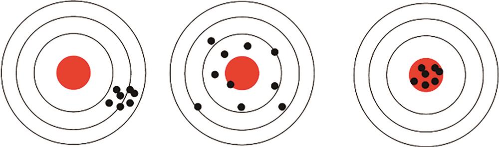
Fig. 1. Precision, accuracy of a LiDAR
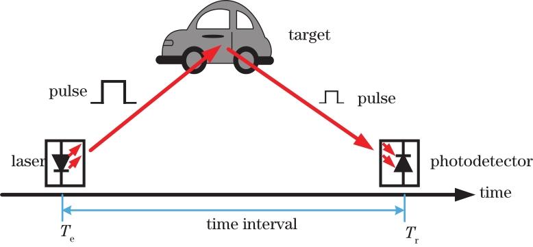
Fig. 2. Schematic of plused TOF LiDAR
Fig. 3. Schematic of RMCW LiDAR
Fig. 4. Principle of FMCW LiDAR
Fig. 5. Micrograph of the chip and macro pixel layout[42]
Fig. 6. Block-based illumination: concept, transmitter PCB, and CMOS receiver IC[43]
Fig. 7. Micrograph of the chip and macro pixel layout[44]
Fig. 8. 3D image acquisition. (a) Photograph of the measured scene ; (b) flash image[44]
Fig. 9. Solid-state LiDAR system[49]. (a) Diagram; (b) chiplet containing LiDAR system on top of a dime; (c) optical micrograph of the device; (d) packaged system with epoxied fiber
Fig. 10. Real-time data from a 3D LiDAR system consisting raster scanning OPAs, and inset shows scene being raster scanned[50]
Fig. 11. Image of the chip[52]. (a) Illustration and microscope image; (b) illustration and vertical SEM image of III/V on Si device
Fig. 12. Structure of solid-state beam scanner chip[53]. (a) Illustration; (b)SEM image of SOA and TLD cross-section; (c) chip microscope image
Fig. 13. Image of OPA[54]. (a) Optical microscope image; (b) SEM image of a fishbone waveguide grating; (c) SEM image of a chain waveguide grating; (d) TEM image of dual-level misaligned waveguide grating with the cladding removed
Fig. 14. LABS device[58]. (a) Diagram; (b) photo of the 1×16 switch chip
Fig. 15. LABS LiDAR with transceiver array[59]. (a) Schematic diagram ; (b) three-dimensional illustration of an integrated transceiver; (c) cross-sectional diagram of the vertical Ge PD in AA' plane
Fig. 16. Microscopic images of the fabricated FPSA device[62]. (a)Microscopic image of 128 pixel×128 pixel FPSA chip; (b) micro image of grating antenna with column selection switch; (c) micro image of grating antenna with row selection switch
Fig. 17. Solid-state 3D imaging LiDAR[63]. (a) Schematic diagram; (b) structure diagram of transmitter and receiver chip; (c) optical micrograph of the demonstrator chip
Fig. 18. FMCW LiDAR chip[64]
Fig. 19. FMCW LiDAR based on silicon photonic platform[66]. (a) Architecture of the system; (b) mask layout of the chip
|
Table 1. Laser and detector types corresponding to LiDAR wavelength


Set citation alerts for the article
Please enter your email address

© Copyright 2018-2021 | Chinese Laser Press. All Rights Reserved 沪ICP备15018463号-20