• Laser & Optoelectronics Progress
  • Vol. 60, Issue 13, 1316019 (2023)
Kexue Sun1,2,*, Jianglin Li1, Zefeng Chen3, Jianbin Xu4, and Qiang Zhao1
Author Affiliations
  • 1College of Electronic and Optical Engineering & College of Flexible Electronics (Future Technology), Nanjing University of Posts and Telecommunications, Nanjing 210023, Jiangsu, China
  • 2Nation-Local Joint Project Engineering Laboratory of RF Integration & Micropackage, Nanjing 210023, Jiangsu, China
  • 3School of Optoelectronic Science and Engineering, Soochow University, Suzhou 215006, Jiangsu, China
  • 4Electronics Engineering Department, The Chinese University of Hong Kong, Hong Kong 999077, China
  • show less
    DOI: 10.3788/LOP230432 Cite this Article Set citation alerts
    Kexue Sun, Jianglin Li, Zefeng Chen, Jianbin Xu, Qiang Zhao. High-Performance van der Waals Heterotunneling Device Based on PdSe2/InSe[J]. Laser & Optoelectronics Progress, 2023, 60(13): 1316019 Copy Citation Text show less
    Schematic diagram and optical microscope image of PdSe2/InSe vertical heterostructure
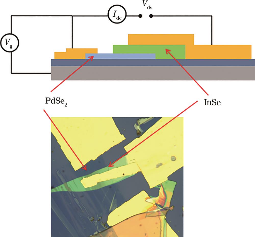
    Fig. 1. Schematic diagram and optical microscope image of PdSe2/InSe vertical heterostructure
    Electrical properties of PdSe2. (a) Relationship between gate voltage and drain current; (b) relationship between drain voltage and drain current
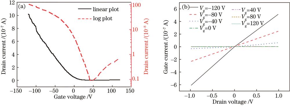
    Fig. 2. Electrical properties of PdSe2. (a) Relationship between gate voltage and drain current; (b) relationship between drain voltage and drain current
    Electron and hole mobility and on/off ratio of PdSe2 devices measured at room temperature in relation to wafer thickness
    Fig. 3. Electron and hole mobility and on/off ratio of PdSe2 devices measured at room temperature in relation to wafer thickness
    I-V characteristics of PdSe2/InSe van der Waals heterostructures at different gate voltages
    Fig. 4. I-V characteristics of PdSe2/InSe van der Waals heterostructures at different gate voltages
    Comparison of reverse rectifier ratio of different reverse diodes made from traditional massive materials Si, GaAs, and GaN with two-dimensional heterogeneous structures WSe2/SnSe2, MoS2/BP, and WSe2/MoS2[21-23]
    Fig. 5. Comparison of reverse rectifier ratio of different reverse diodes made from traditional massive materials Si, GaAs, and GaN with two-dimensional heterogeneous structures WSe2/SnSe2, MoS2/BP, and WSe2/MoS2[21-23]
    AFM and KPFM images of the junction barrier at van der Waals heterojunction interface of PdSe2/InSe
    Fig. 6. AFM and KPFM images of the junction barrier at van der Waals heterojunction interface of PdSe2/InSe
    Material thickness
    Fig. 7. Material thickness
    Work function of the junction
    Fig. 8. Work function of the junction
    Band distribution of Au, InSe, and PdSe2 before contact
    Fig. 9. Band distribution of Au, InSe, and PdSe2 before contact
    I-V characteristics and energy band diagrams of PdSe2/InSe van der Waals heterojunction devices with different bias voltages and gate voltages. (a) I-V characteristics of PdSe2/InSe van der Waals heterojunction devices at -100、100 V gate voltages; (b) energy band diagrams of devices at -100 V gate voltage; (c) energy band diagrams of devices at 100 V gate voltage
    Fig. 10. I-V characteristics and energy band diagrams of PdSe2/InSe van der Waals heterojunction devices with different bias voltages and gate voltages. (a) I-V characteristics of PdSe2/InSe van der Waals heterojunction devices at -100、100 V gate voltages; (b) energy band diagrams of devices at -100 V gate voltage; (c) energy band diagrams of devices at 100 V gate voltage
    Output characteristics of PdSe2/InSe under different laser intensities
    Fig. 11. Output characteristics of PdSe2/InSe under different laser intensities
    Time resolved optical response of the device under 520 nm laser irradiation at Vds=-1 V
    Fig. 12. Time resolved optical response of the device under 520 nm laser irradiation at Vds=-1 V
    Kexue Sun, Jianglin Li, Zefeng Chen, Jianbin Xu, Qiang Zhao. High-Performance van der Waals Heterotunneling Device Based on PdSe2/InSe[J]. Laser & Optoelectronics Progress, 2023, 60(13): 1316019
    Download Citation