• Laser & Optoelectronics Progress
  • Vol. 62, Issue 3, 0304001 (2025)
Han Xu1,*, Kexue Sun1,2, and Rongqing Xu1,2
Author Affiliations
  • 1College of Electronic and Optical Engineering & College of Flexible Electronics (Future Technology), Nanjing University of Posts and Telecommunications, Nanjing 210023, Jiangsu , China
  • 2National and Local Joint Engineering Laboratory of RF Integration and Micro-Assembly Technology, Nanjing 210023, Jiangsu , China
  • show less
    DOI: 10.3788/LOP241182 Cite this Article Set citation alerts
    Han Xu, Kexue Sun, Rongqing Xu. Performance of Metal-Semiconductor-Metal Photodetector Based on LSPR Effect[J]. Laser & Optoelectronics Progress, 2025, 62(3): 0304001 Copy Citation Text show less
    Schematic diagram of 3D simulation structure. (a) Periodic array of hexagonal gold nanowire; (b) schematic diagram of a single cycle interface
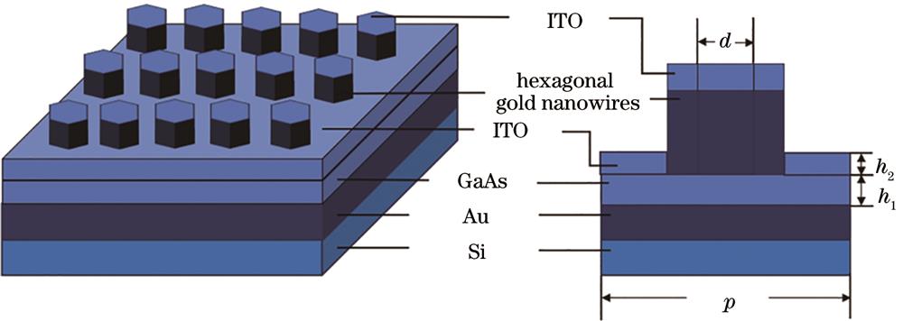
    Fig. 1. Schematic diagram of 3D simulation structure. (a) Periodic array of hexagonal gold nanowire; (b) schematic diagram of a single cycle interface
    Electric field intensity diagrams at the peak of absorption curve for devices with different GaAs thicknesses. (a) GaAs thickness is 10 nm; (b) GaAs thickness is 30 nm; (c) GaAs thickness is 50 nm
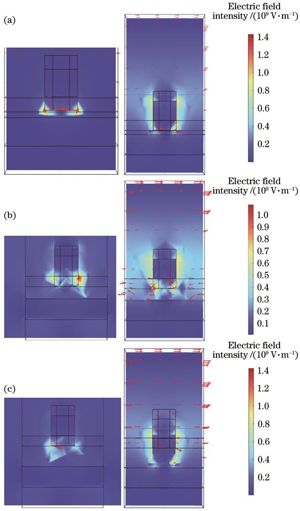
    Fig. 2. Electric field intensity diagrams at the peak of absorption curve for devices with different GaAs thicknesses. (a) GaAs thickness is 10 nm; (b) GaAs thickness is 30 nm; (c) GaAs thickness is 50 nm
    Absorptivity curves of device under different thicknesses of ITO. (a) GaAs thickness of 10 nm; (b) GaAs thickness of 50 nm
    Fig. 3. Absorptivity curves of device under different thicknesses of ITO. (a) GaAs thickness of 10 nm; (b) GaAs thickness of 50 nm
    Variation in absorptivity of device with diameters of gold nanowire
    Fig. 4. Variation in absorptivity of device with diameters of gold nanowire
    Variation in device absorptivity under different incidence angles in TE polarization state
    Fig. 5. Variation in device absorptivity under different incidence angles in TE polarization state
    Variation in responsivity and photocurrent with bias voltage
    Fig. 6. Variation in responsivity and photocurrent with bias voltage
    ParameterNumerical value
    GaAs permittivity12.9
    GaAs band gap /eV1.42
    GaAs electron affinity /eV4.07
    GaAs carrier lifetime /psElectron: 0.1;hole: 0.4
    GaAs mobility /(cm2·v-1·s-1Electron: 400;hole: 100
    GaAs conductivity/(s·m-11.1×103
    N_type doping /cm-31×1015
    Vacuum wave impedance /Ω377
    Temperature /K300
    Auger electron coefficient /(cm6·s-17×10-30
    Auger hole coefficient /(cm6·s-17×10-30
    Bias voltage /V5
    Incident light power /mW10
    Incident wavelength /nm1280
    Resistivity coefficient /(Ω·m25×10-6
    Table 1. Electrical and optical input parameters in the simulation[17-18]