• Photonics Research
  • Vol. 13, Issue 4, 1021 (2025)
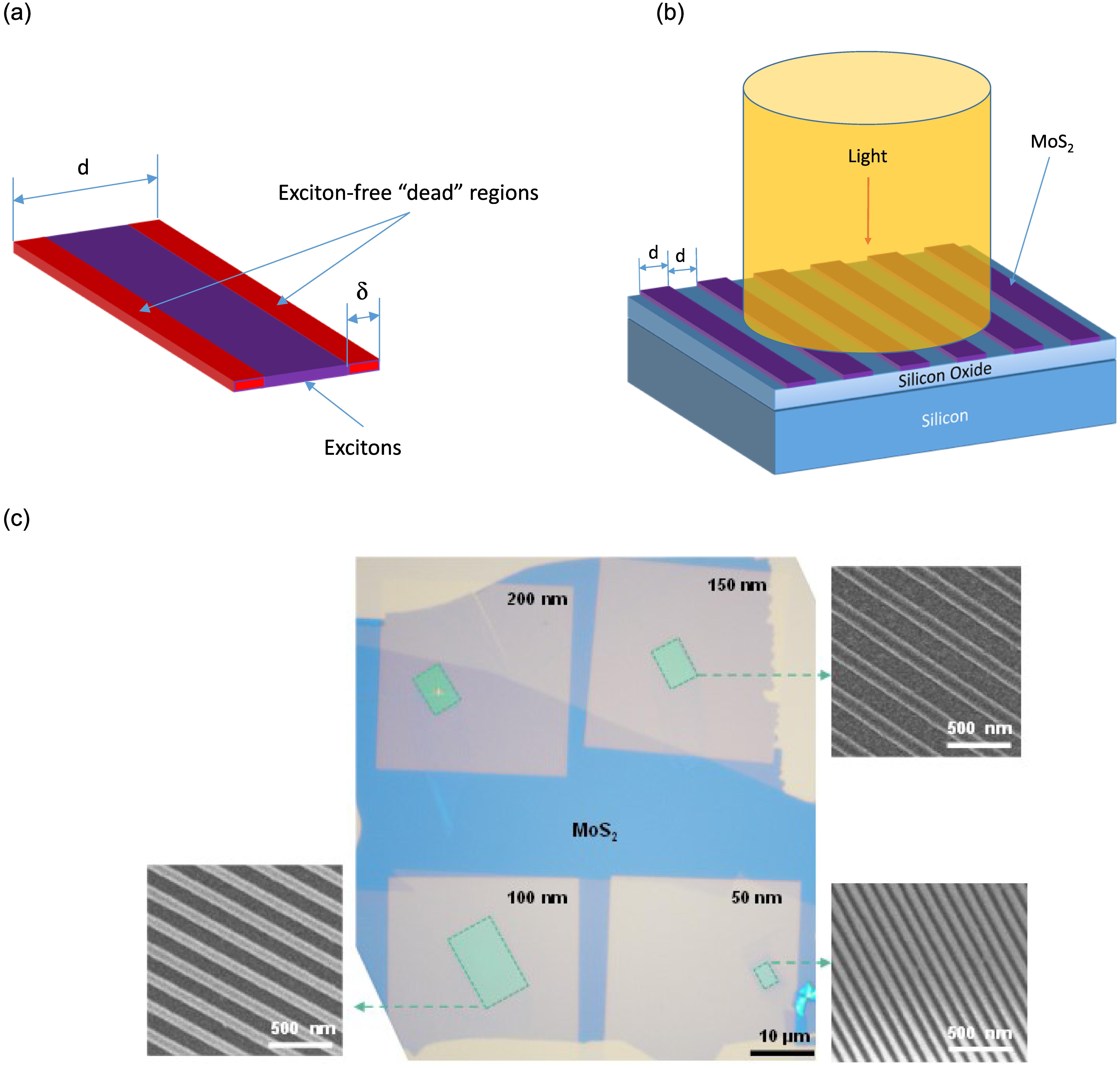
V. G. Kravets1, Zhaolong Chen2,3, Yashar Mayamei1, K. S. Novoselov2, and A. N. Grigorenko1,*
Author Affiliations
  • 1Department of Physics and Astronomy, University of Manchester, Manchester M13 9PL, UK
  • 2Institute for Functional Intelligent Materials, National University of Singapore, Singapore 117544, Singapore
  • 3School of Advanced Materials, Peking University Shenzhen Graduate School, Shenzhen 518055, China
  • show less
    DOI: 10.1364/PRJ.537107 Cite this Article Set citation alerts
    V. G. Kravets, Zhaolong Chen, Yashar Mayamei, K. S. Novoselov, A. N. Grigorenko, "Bilayer MoS2 nanoribbons: observation of optically inactive “exciton-free” regions and electrical gating of optical response," Photonics Res. 13, 1021 (2025) Copy Citation Text show less
    MoS2 nanoribbons and the “dead” exciton regions. (a) Typical MoS2 nanoribbon with “dead” exciton regions shown as the red strips. (b) Schematic of measurements and samples. (c) Optical image of studied samples along with SEM images of bilayer MoS2 nanoribbons with d=50 nm, 100 nm, 150 nm, and 200 nm.
    Fig. 1. MoS2 nanoribbons and the “dead” exciton regions. (a) Typical MoS2 nanoribbon with “dead” exciton regions shown as the red strips. (b) Schematic of measurements and samples. (c) Optical image of studied samples along with SEM images of bilayer MoS2 nanoribbons with d=50  nm, 100 nm, 150 nm, and 200 nm.
    Comparison of MoS2 nanoribbons. (a) Normal reflection from d=50 nmMoS2 nanoribbons relative to reflection from d=150 nmMoS2 nanoribbons of the same 50% filling factor for two polarizations. (b) PL intensities for the same set of nanoribbons as in (a).
    Fig. 2. Comparison of MoS2 nanoribbons. (a) Normal reflection from d=50  nmMoS2 nanoribbons relative to reflection from d=150  nmMoS2 nanoribbons of the same 50% filling factor for two polarizations. (b) PL intensities for the same set of nanoribbons as in (a).
    Gating of MoS2 nanoribbons. (a) Electrical scheme for gating. (b) Top view of a studied structure with a light beam position. (c) Normal reflection of d=50 nm bilayer MoS2 nanoribbons relative to the substrate reflection as a function of gating voltage in the case where the source and the drain are both grounded. No gating is observed. (d) Normal reflection of d=150 nm bilayer MoS2 nanoribbons relative to the substrate reflection as a function of gating voltage in the case where the source and the drain are both grounded. No gating is observed. (e) Normal reflection of d=50 nm bilayer MoS2 nanoribbons relative to the reflection at zero gating voltage with Vs=−2 V and Vd=0. Note the quadratic nature of gating shown in the top inset where the change of reflection at the A exciton position is plotted as a function of gating voltage. (f) Normal reflection of d=150 nm bilayer MoS2 nanoribbons relative to the reflection at zero gating voltage with Vs=−2 V and Vd=0. Note the absence of gating for d=150 nm bilayer MoS2 nanoribbons.
    Fig. 3. Gating of MoS2 nanoribbons. (a) Electrical scheme for gating. (b) Top view of a studied structure with a light beam position. (c) Normal reflection of d=50  nm bilayer MoS2 nanoribbons relative to the substrate reflection as a function of gating voltage in the case where the source and the drain are both grounded. No gating is observed. (d) Normal reflection of d=150  nm bilayer MoS2 nanoribbons relative to the substrate reflection as a function of gating voltage in the case where the source and the drain are both grounded. No gating is observed. (e) Normal reflection of d=50  nm bilayer MoS2 nanoribbons relative to the reflection at zero gating voltage with Vs=2  V and Vd=0. Note the quadratic nature of gating shown in the top inset where the change of reflection at the A exciton position is plotted as a function of gating voltage. (f) Normal reflection of d=150  nm bilayer MoS2 nanoribbons relative to the reflection at zero gating voltage with Vs=2  V and Vd=0. Note the absence of gating for d=150  nm bilayer MoS2 nanoribbons.
    Surface-state-induced band bending in MoS2 nanoribbons.
    Fig. 4. Surface-state-induced band bending in MoS2 nanoribbons.
    A and B excitons in monolayer and bilayer MoS2. (a) Bandgap structure of a MoS2 monolayer. A and B denote the excitonic transitions (∼1.85 eV for A and ∼2 eV for B). The yellow area corresponds to the electrons induced by a gating voltage. (b) Bandgap structure of a MoS2 bilayer. A and B denote the excitonic transitions. The yellow area corresponds to the electrons induced by a gating voltage.
    Fig. 5. A and B excitons in monolayer and bilayer MoS2. (a) Bandgap structure of a MoS2 monolayer. A and B denote the excitonic transitions (1.85  eV for A and 2  eV for B). The yellow area corresponds to the electrons induced by a gating voltage. (b) Bandgap structure of a MoS2 bilayer. A and B denote the excitonic transitions. The yellow area corresponds to the electrons induced by a gating voltage.
    V. G. Kravets, Zhaolong Chen, Yashar Mayamei, K. S. Novoselov, A. N. Grigorenko, "Bilayer MoS2 nanoribbons: observation of optically inactive “exciton-free” regions and electrical gating of optical response," Photonics Res. 13, 1021 (2025)
    Download Citation