
Futong SUN, Aihu FENG, Bingbing CHEN, Yun YU, Hong YANG. Effect of Copper Pretreatment on Growth of Graphene Films by Chemical Vapor Deposition [J]. Journal of Inorganic Materials, 2020, 35(10): 1177
- Journal of Inorganic Materials
- Vol. 35, Issue 10, 1177 (2020)
Abstract
In 2004, Geim and Novoselov[
Up to now, there have been a variety of methods for preparing the graphene materials, mainly including the mechanical exfoliation[
The substrate pretreatment can significantly reduce the catalyst surface defects and impurities [
1 Experimental
1.1 Materials
The isopropyl alcohol, anhydrous ethanol, concentrated sulfuric acid, phosphoric acid and hydrochloric acid were purchased from Sinopharm Chemical Reagent Co., Ltd. (China). The polyethylene glycol, and glycerol were purchased from Shanghai Titan Chemical Co., Ltd. (China). The tributyl phosphate was purchased from Aladdin reagent Co., Ltd. (China), and the copper foil (purity 99.9%, thickness 100 μm) was from Chinalco Luoyang Copper Industry Co., Ltd. (China).
1.2 Pretreatment of copper substrates
In this work, different methods are used to pretreat copper substrate. The untreated copper foil was respectively washed in isopropyl alcohol, absolute ethanol, and deionized water via an ultrasonic for about 10 min. Then, 1) Etching treatment with hydrochloric acid. The sonicated copper foil was placed in 10% hydrochloric acid solution for 2 min, then rinsed with deionized water, and blown dry with nitrogen. 2) Hydrochloric acid etching and electrochemical polishing. Some copper foils etched by hydrochloric acid were furtherly electrochemically polished. The electropolishing time was set to 8 min and voltage to 8 V. The polishing liquid consisted of 100 g of phosphoric acid, 30 g of sulfuric acid, 5 g of hydrochloric acid, 8 g of polyethylene glycol, 5 g of glycerin, 25 g of deionized water, and 1 g of tributyl phosphate. 3) Etching treatment with passivation paste. The surface of copper foil was carefully scrubbed with the passivation paste, and the scrubbing time was set to 2 min. 4) Passivation paste etching and electrochemical polishing. A portion of copper foils treated with the passivation paste were subjected to electrochemical polishing treatment.
1.3 Graphene growth by CVD
The pretreated copper foil was placed in a horizontal quartz tube furnace (inner diameter of 100 mm). The system was evacuated to about 1.33 Pa, and then filled with 200 sccm of argon to atmospheric pressure. Argon (Ar, 99.999% purity) and 100 sccm hydrogen (H2, 99.999% purity) gas mixture was introduced for 10 min, then the temperature program started. When the temperature and pressure reach the desired values, methane was introduced (from 0.5 sccm to 5.0 sccm). The growth temperature was set to 1060 ℃, and the process was carried out for 25 min. Then, it was cooled to room temperature under an atmosphere of argon and hydrogen.
1.4 Characterization
The surface morphology of copper substrates and graphene samples were examined by an optical microscope (OM, DM2500M, Leica Instruments Co., Ltd.) and a scanning electron microscope (SEM, Hitach S-4800, Bruker). The graphene structure was tested by Raman spectroscopy ( XploRA PLUS, HORIBA, Japan).
2 Results and discussion
2.1 Different pretreatment on copper substrate
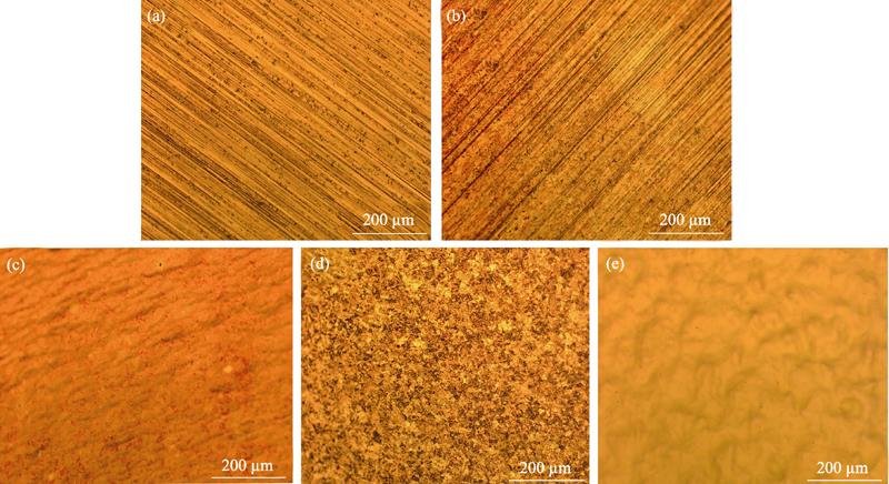
The copper substrates were treated by different methods, and the optical microscope images of different samples are shown in Fig. 1. As can be seen from Fig. 1(a), there are a large number of streaks and impurity defects on the surface of the untreated copper foil. From Fig. 1(b), the surface morphology of the copper foil does not change much, and the surface still has streaks and defects after etching with hydrochloric acid for 20 h. Therefore, the dilute hydrochloric acid etching treatment does not give the copper foil a smooth surface. When the copper foil is further processed by electrochemical polishing, the surface morphology of copper foil is changed significantly in Fig. 1(c). The original stripe disappears and the surface is more smooth. Fig. 1(d) is the photomicrograph of the copper foil treated with passivation paste. It can be seen that the corrosion effect is obvious and the surface morphology is completely changed, but the surface exhibits loose and rough appearance. Then the copper foil treated by the passivation paste is furtherly subjected to electrochemical polishing treatment. Surprisingly, the flatness and smoothness of the copper foil substrate are significantly improved, and the mirror effect is macroscopically achieved as shown in Fig. 1(e). So the combination of the passivation paste pickling and electrochemical polishing is an effective method for treating copper substrates.
![]()
Figure 1.OM images of different copper substrates(a) Untreated copper substrate; (b) Hydrochloric acid etching treatment; (c) Hydrochloric acid etching and electrochemical polishing treatment; (d) Passivation paste etching; (e) Passivation paste etching and electrochemical polishing treatment
2.2 Effect of electrochemical polishing voltage and polishing time
In order to explore the process parameters of electrochemical polishing, the effect of polishing voltage and polishing time were studied. As shown in Fig. 2, three polishing voltages, 1.2, 4.0 and 8.0 V, were selected. It can be seen from Fig. 2(a1-a4) that when the polishing voltage is set to 1.2 V, electrochemical polishing treatment has little effect on the copper foil. There are still some defects such as streaks and pits on the surface of copper foils even if the polishing time increases to 40 min. When voltage is 4 V, the surface of the copper foil treated for 10 min changes significantly in Fig. 2(b1), and the streaks become shallow. With the polishing time increasing to 30 min, the streaks and defects on copper surface are completely removed as shown in Fig. 2(b3). However, the excessive corrosion pits appear if polishing time is up to 40 min. In Fig. 2(b4), it can be demonstrated that there are some corrosion pits on the surface of the copper foil. As the polishing voltage increasing to 8 V, the polishing time also has great influence on copper surface morphology. When the polishing time is 8 min, the surface of the copper foil substrate is flat and smooth as shown in Fig. 2(c1). The surface smoothness is improved significantly with the polishing time increasing, but excessive prolonging polishing time easily causes corrosion (Fig. 2(c2-c4)).
![]()
Figure 2.OM images of copper substrates electrochemical polished with different voltages and time(a1) 1.2 V/10 min; (a2) 1.2 V/20 min; (a3) 1.2 V/30 min; (a4) 1.2 V/40 min; (b1) 4 V/10 min; (b2) 4 V/20 min; (b3) 4 V/30 min; (b4) 4 V/40 min; (c1) 8 V/6 min; (c2) 8 V/8 min; (c3) 8 V/10 min; (c4) 8 V/12 min
Therefore, the copper foil cannot be significantly polished when the polishing voltage is too low, while the excessive polishing time causes excessive polishing with high voltage. Based on the results, the appropriate polishing voltage and time are set as 8 V and 8 min, respectively.
2.3 Effect of annealing temperature
In the growing process of graphene, the grain size and uniformity of copper catalyst have great influence on graphene quality and size. The temperature is a very important factor, and the annealing treatment can signifycantly improve the surface morphology of the copper foil substrate. The copper foils were annealed at different temperatures for 30 min. It can be seen from Fig. 3(a) that when the annealing is performed at 800 ℃ for 30 min, the grain is less than 100 μm in size and ununiform. As the annealing temperature rises to 900 ℃, the surface morphology of the copper foil substrate is slightly changed, and some grain become larger (~200 μm). But the annealing effect is still poor, and grain size is still uneven. When the annealing temperature is increased to 1000 and 1060 ℃, the grain size of the copper foil is larger and the uniformity is significantly improved, as shown in Fig. 3(c, d).
![]()
Figure 3.OM images of copper substrates annealed at different temperatures for 30 min (a) 800 ℃; (b) 900 ℃; (c) 1000 ℃; (d) 1060 ℃
2.4 Effect of annealing time
In addition to annealing temperature, the annealing time also seriously affects copper grain size and its uniformity. When the annealing temperature is 1000 ℃ with no holding time, the grain is unevenly distributed with dimension less than 200 μm, as shown in Fig. 4(a). However, the grain becomes significantly larger as the annealing time is kept at 30 min, and most of the grains exceed 200 μm with improved uniformity (Fig. 4(b)). With the annealing time increasing to 90 or 120 min, Cu grains continue to increase (>400 μm), while the number of grains decreases (Fig. 4(c, d)). However, too long annealing time can increase energy cost. Considering the results from Fig. 3 and Fig. 4, the copper foil substrate with larger grain size and uniform distribution can be obtained by annealing at 1000 ℃ for 30 min.
![]()
Figure 4.OM images of copper substrates annealed at 1000 ℃ for different time (a) 0; (b) 30 min; (c) 90 min; (d) 120 min
2.5 Graphene characterization
SEM image of graphene sample by CVD growth is shown in Fig. 5. Two regions, gray and dark gray area are clearly visible, indicating that different layers of graphene are grown. In order to analyze the quality of the prepared graphene, the graphene in different regions are characterized by the Raman spectra (Fig. 6). The D peak in Raman spectra represents the defect peak of graphene, while the G peak represents the characteristic peak of carbon sp2, reflecting the crystallinity and symmetry. 2D is the second-order Raman scattering peak of the region boundary phonon, which is used to determine the existence of graphene. So the IG/ID demonstrates the degree of defect of the graphene crystal, and I2D/IG represents graphene layer. Fig. 6(a) is the Raman spectrum of the quartz substrate. The quartz substrate can produce a light scattering effect to cause characteristic peaks other than graphene in Fig. 6(b, c). Compared with the Raman spectrum of the graphene sample in gray area, the D band intensity of graphene in dark gray area is lower, while the 2D band intensity is significantly higher, as show in Fig. 6(b, c). In addition, the ID /IG is slightly decreased, and the I2D/IG is obviously increased in Table 1. Therefore, the graphene in dark gray area has fewer defects and better quality.
![]()
Figure 5.SEM image of graphene sample
![]()
Figure 6.Raman spectra of quartz substrate (a), graphene sample in gray area (b), and graphene sample in dark gray area (c)
3 Conclusion
The effects of different pretreatment on the surface morphology of copper substrates were studied. It can be found that the combined treatment of passivation paste pickling and electrochemical polishing can effectively remove surface defects on copper substrates. The influence of polishing process and annealing process parameters on the copper substrate are systematically demonstrated, and a process for preparing high-quality graphene by CVD is developed. According to the SEM image and Raman spectrum, the graphene film prepared in this work is few-layer, large-size, high-quality. It is worth emphasizing that the copper foil used in this work is the common copper foil, and its purity is only 99.9%. Overall, our work provides a novel method for large-scale preparation of high-quality graphene.
| Area | D band/cm-1 | G band/cm-1 | 2D band/cm-1 | ||
|---|---|---|---|---|---|
| Gray area | 1354 | 1581 | 2697 | 0.57 | 0.83 |
| Dark gray area | 1354 | 1592 | 2684 | 0.26 | 1.29 |
Table 1.
Comparison of the Raman characteristic peak in different graphene areas
References
[5] E GALASHEV A. Computer simulation of the thermal stability of nickel films on two-layer graphene. High Temperature, 52, 633-639(2014).
[6] J ZENG, X JI X, H MA Y et al. 3D graphene fibers grown by thermal chemical vapor deposition. Advanced Materials, 30, 1705380(2018).
[7] G LIM, D KIHM K, G KIM H et al. Enhanced thermoelectric conversion efficiency of cvd graphene with reduced grain sizes. Nanomaterials, 8, 557(2018).
[11] N ZHANG, K ZHAO X, B FU X et al. Preparation and characterization of polyamide-6/reduced graphene oxide composite microspheres. ChemistrySelect, 4, 11294-11301(2019).
[12] N MAHAMAI, T PROM-ANAN, T SARAKONSRI. Preparation and characterization of platinum alloy catalysts supported on
[13] J TIAN, L GUO, L YIN X et al. The liquid-phase preparation of graphene by shear exfoliation with graphite oxide as a dispersant. Materials Chemistry and Physics, 223, 1-8(2019).
[14] D ZHANG D, L FU, L LIAO et al. Preparation, characterization, and application of electrochemically functional graphene nanocomposites by one-step liquid-phase exfoliation of natural flake graphite with methylene blue. Nano Research, 5, 875-887(2012).
[15] T MA, H ARIGA, S TAKAKUSAGI et al. Smooth epitaxial copper film on sapphire surface suitable for high quality graphene growth. Thin Solid Films, 646, 12-16(2018).
[16] C MATTEVI, H KIM, M CHHOWALLA. A review of chemical vapour deposition of graphene on copper. Journal of Materials Chemistry, 21, 3324-3334(2011).
[17] P FANG L, W YUAN, B WANG et al. Growth of graphene on Cu foils by microwave plasma chemical vapor deposition: the effect of
[18] D MENDOZA C, G CALDAS P, L FREIRE F et al. Growth of single-layer graphene on Ge (100) by chemical vapor deposition. Applied Surface Science, 447, 816-821(2018).
[19] H WANG, Z WANG G, F BAO P et al. Controllable synthesis of submillimeter single-crystal monolayer graphene domains on copper foils by suppressing nucleation. Journal of the American Chemical Society, 134, 18476-18476(2012).
[20] X ZHAO, L GOU. Comparative analysis of graphene grown on copper and nickel sheet by microwave plasma chemical vapor deposition. Vacuum, 153, 48-52(2018).
[22] Z XU. Heat transport in low-dimensional materials: a review and perspective. Theoretical and Applied Mechanics Letters, 6, 113-121(2016).
[23] M YARIFARD, J DAVOODI, H RAFII-TABAR. Computation of the thermal resistance in graphene sheets with a rectangular hole. Computational Materials Science, 126, 29-34(2017).
[28] D HU X, M ZHANG, Y XUE Z et al. The effect of copper pretreatment on graphene synthesis by ion implantation into Ni/Cu substrate. Semiconductor Science and Technology, 33, 074001(2018).
[29] H JEONG, T HWANG W, Y SONG et al. Highly uniform monolayer graphene synthesis


Set citation alerts for the article
Please enter your email address

© Copyright 2018-2021 | Chinese Laser Press. All Rights Reserved 沪ICP备15018463号-20