• Infrared and Laser Engineering
  • Vol. 53, Issue 7, 20240136 (2024)
Lixia ZHENG1, Wangqiao YOU1, Kang HU1, Jin WU1..., Weifeng SUN1 and Xingye ZHOU2,*|Show fewer author(s)
Author Affiliations
  • 1School of Integrated Circuits, Southeast University, Wuxi 214125, China
  • 2China Electronics Technology Group Corporation 13th Research Institute (CETC 13), Shijiazhuang 050051, China
  • show less
    DOI: 10.3788/IRLA20240136 Cite this Article
    Lixia ZHENG, Wangqiao YOU, Kang HU, Jin WU, Weifeng SUN, Xingye ZHOU. Fast active-passive mixed quenching circuit applied to SPAD array[J]. Infrared and Laser Engineering, 2024, 53(7): 20240136 Copy Citation Text show less
    Circuit architecture diagram
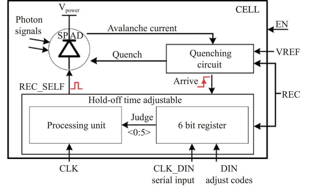
    Fig. 1. Circuit architecture diagram
    Timing diagram of the circuit nodes
    Fig. 2. Timing diagram of the circuit nodes
    (a) Passive quenching circuit structure; (b) Active-passive mixed quenching circuit structure
    Fig. 3. (a) Passive quenching circuit structure; (b) Active-passive mixed quenching circuit structure
    Transient response of the mixed quenched SPAD
    Fig. 4. Transient response of the mixed quenched SPAD
    (a) Equivalent circuit diagram of the quenching circuit with \begin{document}$ {R}_{{\mathrm{S}}} $\end{document} in passive quenching stage; (b) Circuit without \begin{document}$ {R}_{{\mathrm{S}}} $\end{document}
    Fig. 5. (a) Equivalent circuit diagram of the quenching circuit with Unknown environment 'document' in passive quenching stage; (b) Circuit without Unknown environment 'document'
    Simulated dependence of the induction delay time on inductive resistance \begin{document}$ R\mathrm{_S} $\end{document} for different k
    Fig. 6. Simulated dependence of the induction delay time on inductive resistance Unknown environment 'document' for different k
    Simulated dependence of the normalized delay improvement on inductive resistance \begin{document}$ R\mathrm{_S} $\end{document} for k=k2
    Fig. 7. Simulated dependence of the normalized delay improvement on inductive resistance Unknown environment 'document' for k=k2
    Simulated dependence of the “cost performance” on inductive resistance \begin{document}$ R\mathrm{_S} $\end{document} for different k
    Fig. 8. Simulated dependence of the “cost performance” on inductive resistance Unknown environment 'document' for different k
    Quenching circuit structure
    Fig. 9. Quenching circuit structure
    (a) Layout of the proposed circuit; (b) Chip diagram of the detector and circuit connection
    Fig. 10. (a) Layout of the proposed circuit; (b) Chip diagram of the detector and circuit connection
    (a) Measured resetting time of the proposed circuit; (b) Measured quenching time of the proposed circuit
    Fig. 11. (a) Measured resetting time of the proposed circuit; (b) Measured quenching time of the proposed circuit
    PerformanceYearQuenching time/nsResetting time/nsLayout area/μm2
    This work20232.91.75 ns120×100
    Ref.[13]2019<5<3 ns260×138
    Ref.[14]20215.132.36 ns120×86
    Ref.[15]20202.12.8 nsN/A
    Table 1. Comparison of proposed quenching circuit with state-of-art
    Lixia ZHENG, Wangqiao YOU, Kang HU, Jin WU, Weifeng SUN, Xingye ZHOU. Fast active-passive mixed quenching circuit applied to SPAD array[J]. Infrared and Laser Engineering, 2024, 53(7): 20240136
    Download Citation