Xuehao Yu, Xiaodong Fang, Libing You, Yizhe Wang, Molin Liu, Hao Wang. Research progress of excimer laser annealing in semiconductor integrated circuit manufacturing[J]. Infrared and Laser Engineering, 2023, 52(12): 20230285
Search by keywords or author
- Infrared and Laser Engineering
- Vol. 52, Issue 12, 20230285 (2023)
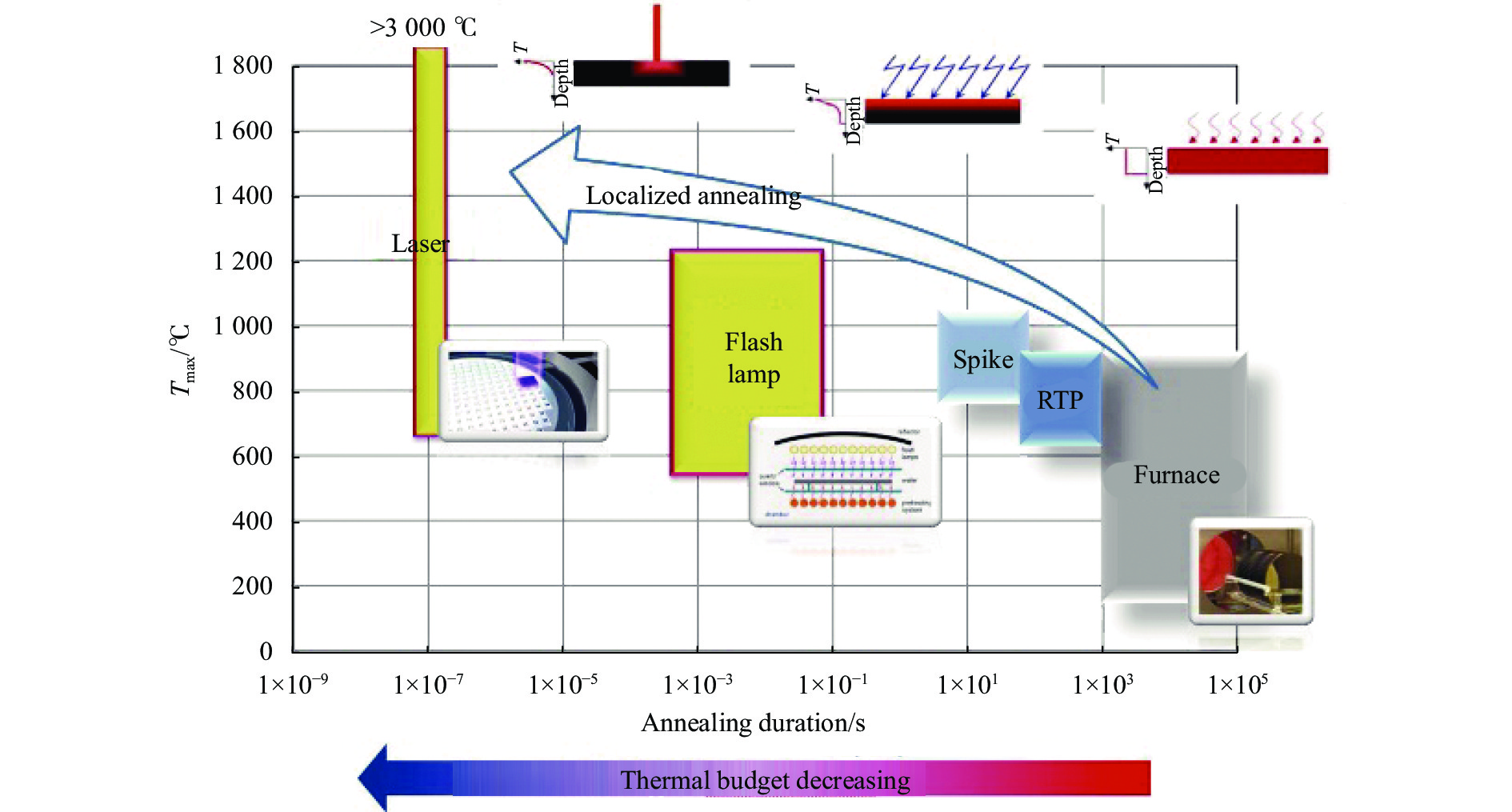
![Schematic diagram about thermal budget evolution[41]](/richHtml/irla/2023/52/12/20230285/img_1.jpg)
Fig. 1. Schematic diagram about thermal budget evolution[41]
![SIMS diagram about laser annealing Ge SIMS diagram in different energy densities[41]](/richHtml/irla/2023/52/12/20230285/img_2.jpg)
Fig. 2. SIMS diagram about laser annealing Ge SIMS diagram in different energy densities[41]
Fig. 3. Contact resistivity of P FinFET with laser annealing[41]
Fig. 4. Laser annealing cross section simulation of nanowire-structured devices[41]
Fig. 5. Process flow for M1 interconnects with melt laser anneal in 14 nm Finfet divice[41]
Fig. 6. 3D sequential integration related problem induction diagram[41]
Fig. 7. Phase field evolution of single pulse ELA process at 0.717 J/cm2, the time interval between the two phase field profiles is 5 ns[65]
Fig. 8. Density field evolution during a single pulse ELA at 0.717 J/cm2[65]
Fig. 9. Surface simulation curve and SIMS curve of As after ten pulses[65]
Fig. 10. Simulation diagram of Si melt depth varying with laser energy density at substrate temperature of 450 ℃[66]
Fig. 11. SIMS diagram of (a) spike annealing and (b) excimer laser annealing[67]
Fig. 12. Effect of different pulse number on junction depth[67]
Fig. 13. Variation of sheet resistance and junction depth with laser energy density[68]
Fig. 14. DXRD curve graph[68]
Fig. 15. Raman spectrum c-Ge : a-Ge ratio chart[69]
Fig. 16. SIMS curves of Sb before and after excimer laser annealing[70]
Fig. 17. SIMS diagram of (a) boron and (b) arsenic[71]
Fig. 18. Heat distribution after 65 ns 308 nm laser irradiation (a) bulk silicon devices and (b) SOI devices[71]
Fig. 19. The effect of laser energy density approaching the full melting threshold on the activation of dopants[72]
Fig. 20. TEM images of materials treated by excimer laser with different energy densities[74]
Fig. 21. (a) Time resolved reflectance (TRR) and laser pulse profile at different laser energy densities; (b) The relationship between reflectance and laser energy density[75]
Fig. 22. TEM images about 30 nm Si0.8Ge0.2 thickness annealed by (a)-(b) 1.59 J/cm2, (c)-(d) 1.80 J/cm2 and (e)-(f) 2.00 J/cm2 exci-mer laser[75]
Fig. 23. (a) Temperature field and (b) time evolution of interconnect structures treated by pulsed laser (ULK/Cu)[77]
Fig. 24. Effect of multiple pulses on sheet resistance at 400 ℃[78]
Fig. 25. TEM images of cross sections of materials subjected to heat annealing at 400 ℃ for 1 hour or excimer laser annealing[78]
Fig. 26. Electron backscatter diffraction pattern of laser annealing And grain size of metal diagram[79]
Fig. 27. Diagram of 3D integrated circuit structure[80]
Fig. 28. TEM comparison of excimer laser annealing device (a) and spike annealing device (b)[81]
Fig. 29. Simulated structure and comparison of absorption power density of two-dimensional structure[82]
Fig. 30. The relationship between temperature and time of interlayer oxides and underlying oxides. T1: the temperature at the upper grid, T2: the temperature at the lower grid, and T3: the temperature at the top of the bulk silicon[82]
Fig. 31. The resistivity of copper interconnection wire changes with laser energy[83]
Fig. 32. The relationship between temperature and time about devices’s a-Si layer and Cu interconnection with different layers of thickness after excimer laser annealing [83]
Fig. 33. Si size with different annealing methods[84]
Fig. 34. Dark field STEM diagrams of (a) full channel device, (b) macaroni-type device, and (c) macaroni-type device with excimer laser annealing[85]
Fig. 36. Drain current statistical distribution and interface traps distribution [85]

Set citation alerts for the article
Please enter your email address


