
Rui Yang, Qianqian Yu, Yiwei Pan, Sihan Chen, Chen Zhang, Hong Ye, Xinyao Zhou, Yangyang Shi, Shuai Wan, Yang Liu, Zhongyang Li. Directional-multiplexing holography by on-chip metasurface[J]. Opto-Electronic Engineering, 2022, 49(10): 220177
- Opto-Electronic Engineering
- Vol. 49, Issue 10, 220177 (2022)
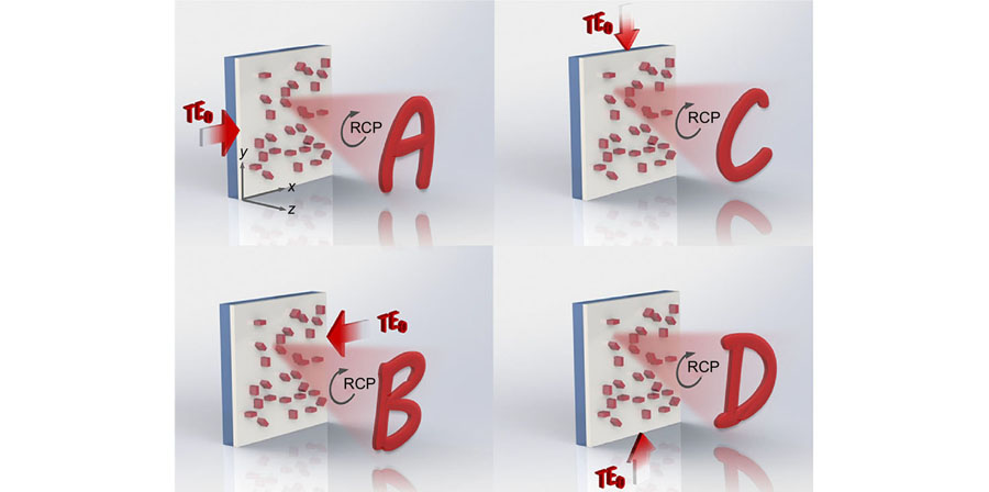
Fig. 1. Schematic diagram of the on-chip four-channel multiplexed holography. Four diverse holographic images (“A/B/C/D”) in the far-field could be displayed by the on-chip metasurface integrated on the waveguide, when the laser source is end-fire coupled into the waveguide along the ±x and ±y directions, respectively

Fig. 2. On-chip metasurface mechanism for controlling the phase of extracted guided waves. (a) Schematic of the unit cell to compose the on-chip metasurface; (b) The principle of guided wave extraction by combining the detour phase and geometric phase; (c) The correspondence between discrete detour phases and the positions of meta-atoms in the unit cell; (d) The relationship between discrete geometric phase delay and the orientation angle of the meta-atoms
Fig. 3. Phase optimization flowchart for the on-chip quad-fold multiplexed holography
Fig. 4. The sample fabrication flow chart of the on-chip quad-fold multiplexing holographic metasurface
Fig. 5. Experimental verification for the on-chip quad-fold holography. (a) The overall SEM image and zoom-in SEM image of the fabricated sample; (b) Optical experimental setup sketch for measuring on-chip quad-fold holography; (c) Target and experimental holograms measured in the area corresponding to the target for guided waves incidence from the ±x/±y direction, respectively


Set citation alerts for the article
Please enter your email address

© Copyright 2018-2021 | Chinese Laser Press. All Rights Reserved 沪ICP备15018463号-20