• Chinese Optics Letters
  • Vol. 15, Issue 2, 021301 (2017)
Mansour Bacha1,2,* and Abderrahmane Belghoraf1
Author Affiliations
  • 1Electronics Department, University of Sciences and Technology of Oran Mohamed Boudiaf, Oran M’Naouer BP 1505, Algeria
  • 2Centre of Satellites Development, Ibn Rochd USTO Oran BP 4065, Algeria
  • show less
    DOI: 10.3788/COL201715.021301 Cite this Article Set citation alerts
    Mansour Bacha, Abderrahmane Belghoraf, "Numerical evaluation of radiation and optical coupling occurring in optical coupler," Chin. Opt. Lett. 15, 021301 (2017) Copy Citation Text show less
    Configuration of the optical coupler to analyze.
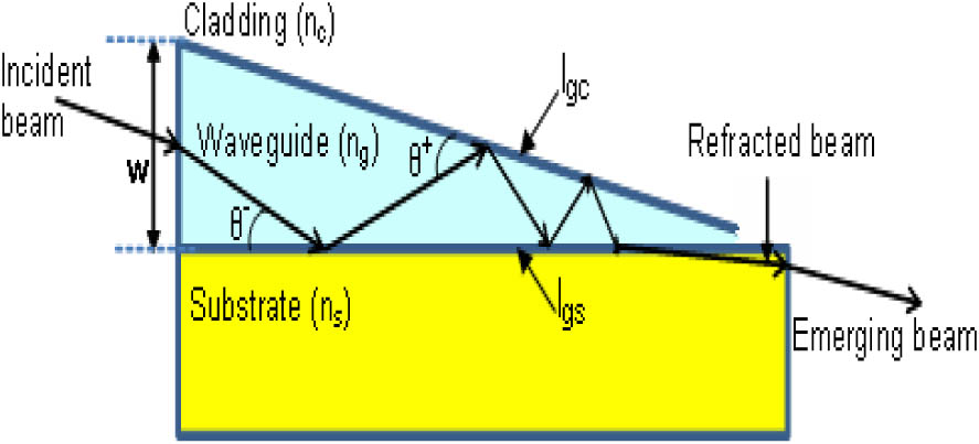
    Fig. 1. Configuration of the optical coupler to analyze.
    Second intrinsic normalized mode (q=2) of a symmetric polymer optical waveguide for the wedge angle a=0.03 rad. The dashed graph represents the normalized intrinsic field at a thickness of W=3 μm, and the solid line represents the intrinsic field at thickness W=0.4, which is lower than the cut-off thickness.
    Fig. 2. Second intrinsic normalized mode (q=2) of a symmetric polymer optical waveguide for the wedge angle a=0.03rad. The dashed graph represents the normalized intrinsic field at a thickness of W=3μm, and the solid line represents the intrinsic field at thickness W=0.4, which is lower than the cut-off thickness.
    Third intrinsic normalized mode (q=3) of a symmetric polymer optical waveguide for the wedge angle a=0.03 rad. The dashed graph represents the normalized intrinsic field at a thickness of W=4 μm, and the solid line represents the field at a thickness of W=0.9, which is lower than the cut-off thickness.
    Fig. 3. Third intrinsic normalized mode (q=3) of a symmetric polymer optical waveguide for the wedge angle a=0.03rad. The dashed graph represents the normalized intrinsic field at a thickness of W=4μm, and the solid line represents the field at a thickness of W=0.9, which is lower than the cut-off thickness.
    Power distribution in the three regions of a symmetric tapered waveguide for the mode q=3 and a wedge angle a=1° for (a) the waveguide AlAsGa/AsGa/AlAsGa and (b) the waveguide SiO2/Si/SiO2.
    Fig. 4. Power distribution in the three regions of a symmetric tapered waveguide for the mode q=3 and a wedge angle a=1° for (a) the waveguide AlAsGa/AsGa/AlAsGa and (b) the waveguide SiO2/Si/SiO2.
    Power distribution in the three regions of a symmetric tapered waveguide for the mode q=3 and a wedge angle a=5° for (a) the waveguide AlAsGa/AsGa/AlAsGa and (b) the waveguide SiO2/Si/SiO2.
    Fig. 5. Power distribution in the three regions of a symmetric tapered waveguide for the mode q=3 and a wedge angle a=5° for (a) the waveguide AlAsGa/AsGa/AlAsGa and (b) the waveguide SiO2/Si/SiO2.