
Hongming Fei, Min Wu, Han Lin, Yibiao Yang, Liantuan Xiao, "Tunable hexagonal boron nitride topological optical delay line in the visible region," Chin. Opt. Lett. 22, 053602 (2024)
- Chinese Optics Letters
- Vol. 22, Issue 5, 053602 (2024)
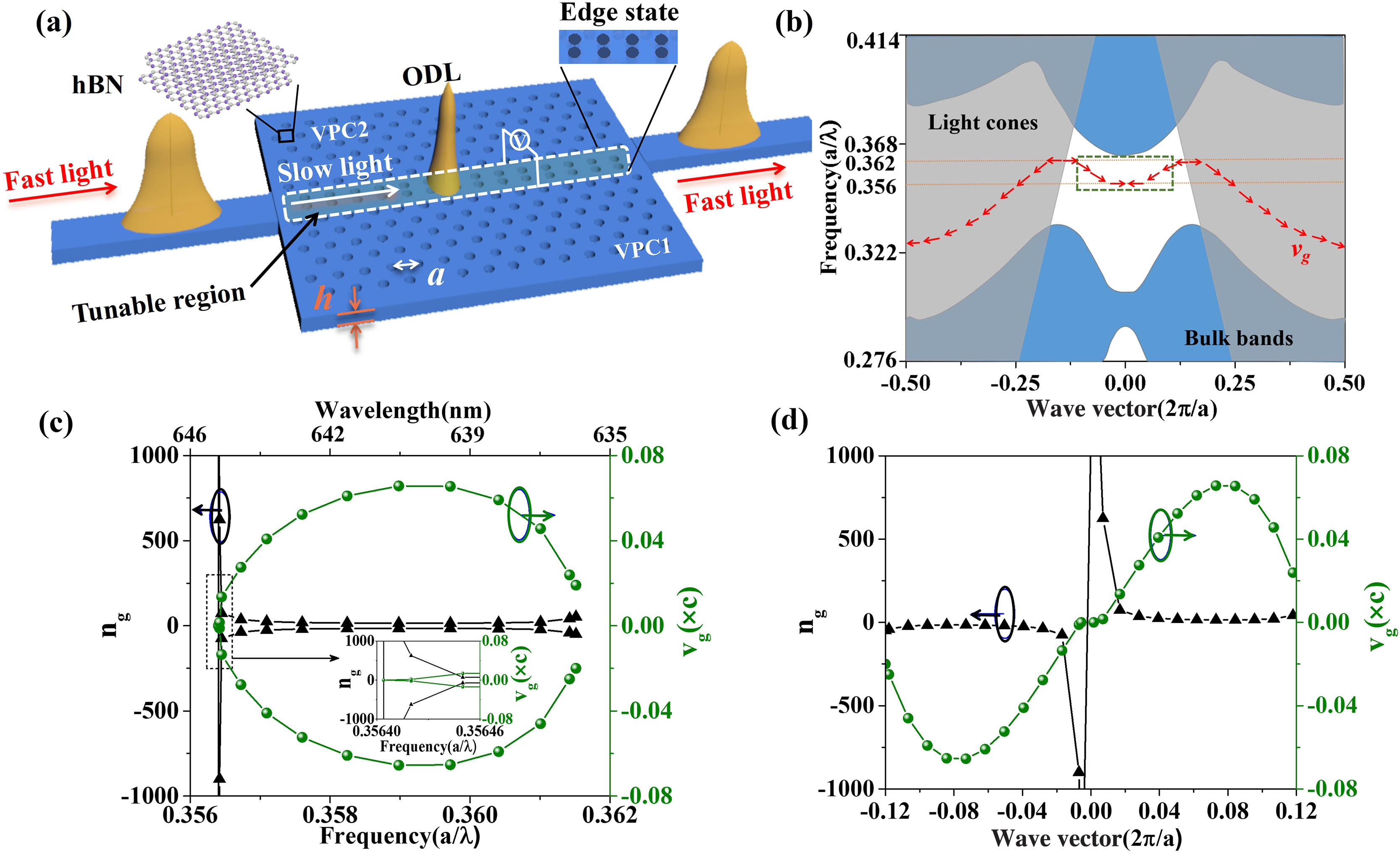
Fig. 1. (a) The schematic diagram of an ODL based on a VPC structure, in which the yellow shadow marks the slow-light waveguide. The red arrows mark the propagation direction of incident light. As the incident light couples into the slow-light waveguide, the effective wavelength is shortened, resulting in a slow group velocity. The inset shows the molecular structure of hBN material. (b) The band diagram of the beard-type boundary. The blue area is the bulk band, and the gray area is the light cone. The two red arrows mark the directions of the vg. (c) The group index (ng) and the group velocity (vg) plots versus wavelength (λ) and frequency. (d) The group index (ng) and the group velocity (vg) plots versus wave vector (k).

Fig. 2. (a) Poynting vector distributions at 645 nm. (b) and (c) Edge state’s electric and magnetic field intensity distributions at 645 nm.
Fig. 3. (a) Schematic diagram of beard-type boundary filled with liquid crystal, where the yellow columns indicate tunable regions; (b) birefringence plot of liquid crystal at different voltages[49]; (c) edge state plots at different voltages; (d) plot of slow-light wavelengths at different voltages.
Fig. 4. (a) Electric field intensity distributions in a straight waveguide at 645 nm; (b)–(d) transmittance spectra of the straight waveguides with different refractive indices; the gray shadow marks the working bandwidth; electric field intensity distributions at 645 nm and transmittance spectra of Z-type [(e) and (f)] and Ω-type waveguides [(g) and (h)]; the gray region represents the unidirectional transmission working bandwidth, where the forward transmittance is higher than −2.5 dB.
Fig. 5. (a) Optical delay times of the Ω-type waveguides with different refractive indices; (b) optical delay times of the Ω-type waveguides filled with liquid crystals at different voltages at 667 nm.


Set citation alerts for the article
Please enter your email address

© Copyright 2018-2021 | Chinese Laser Press. All Rights Reserved 沪ICP备15018463号-20