Xinyi Wang, Jiangbing Du, Weihong Shen, Ke Xu, Zuyuan He, "High-density MDM-WDM silicon photonic transmitter chiplet based on MRMs and dual-mode GC for 4 × 56 Gbps 3D co-packaged optical interconnects," Chin. Opt. Lett. 22, 120001 (2024)
Copy Citation Text
【AIGC One Sentence Reading】:A 4×56 Gbps silicon photonic MDM-WDM transmitter chiplet, using MRMs & dual-mode GC, demonstrates high-density 3D co-packaged optical interconnects.
【AIGC Short Abstract】:A 1.65 mm² silicon photonic chiplet integrating MDM-WDM technology uses add-drop micro-ring modulators for electro-optic modulation and two-wavelength multiplexing. With a dual-mode grating coupler, it achieves high chip-to-fiber coupling efficiency, supporting 4 × 56 Gbps signaling, ideal for high-density 3D co-packaged optical interconnects.
Note: This section is automatically generated by AI . The website and platform operators shall not be liable for any commercial or legal consequences arising from your use of AI generated content on this website. Please be aware of this.
Abstract
In this Letter, a four-channel silicon photonic mode-division-multiplexing (MDM) and wavelength-division multiplexing (WDM) transmitter chiplet is proposed over a 1.65 mm2 footprint, utilizing add-drop micro-ring modulators to simultaneously achieve electro-optic modulation and two-wavelength multiplexing. A dual-mode grating coupler with a side-distributed Bragg reflector for equalized two-mode coupling is realized with high chip-to-fiber coupling efficiency, so as to support the MDM optical fiber interface. A high data rate of up to 4 × 56 Gbps signaling is experimentally demonstrated, featuring applications like 200G quad small form-factor pluggable (QSFP) transceivers and indicating significant potential for high-density and large-capacity 3D co-packaged optical interconnects through flip-chip-based electronic-photonic packaging.
With exponentially growing data traffic in data centers (DCs) and high-performance computing (HPC) systems due to the rise of 5G, IoT, AI, and other applications, silicon photonics (SiPh)-based optical interconnects have appeared as a promising technology to achieve large communication capacity, featuring high aggregated bandwidth, low power consumption, high-density integration, and complementary metal-oxide-semiconductor (CMOS) compatibility[1–3]. In the past few years, silicon-based optical integrated components involving either passive or active devices[4–7] have been extensively demonstrated in high-speed transmission above 100G for a single channel[8]. On the other hand, multi-channel multiplexing techniques are in high demand for obtaining higher accumulated data rates for practical optical interconnect scenarios.
Wavelength-division multiplexing (WDM) is primarily developed to expand the communication capacity, which achieves parallel signal transmission by independently encoding data on multiple wavelength channels, thus fully utilizing the wide bandwidth of the optical interconnection medium. In the past decade, silicon photonic WDM transmitters based on Mach–Zehnder modulators (MZMs)[9–11], micro-ring modulators (MRMs)[12–16], and electro-absorption modulators (EAMs)[17] have been extensively demonstrated for large-capacity transmission. However, silicon WDM techniques always impose stricter requirements on multi-wavelength laser sources and wavelength precise controls, increasing the system complexity, power consumption, and cost[18].
To further increase the link bandwidth, other promising dimensions of data transfer, like separate guided modes, can also be utilized for multiplexing[19–22]. Specifically, multiple parallel signal transmission can be carried with a set of orthogonal spatial modes in multimode optical waveguides, and each mode channel can support a full WDM link[23]. Recently, significant progress has been made toward hybrid mode-division-multiplexing (MDM)-WDM silicon photonic-integrated transmitters to fully utilize the wavelength and mode degrees of freedom for significantly extending the data transmission capacity[24,25]. In Ref. [24], an MDM-WDM transmitter employing three wavelengths and two modes is demonstrated with a micro-resonator-based Kerr comb source, a silicon MZM, a micro-ring resonator (MRR)-based wavelength multiplexer (MUXs), and an adiabatic coupler (ADC)-based two-mode multiplexers. An accumulated data rate of 150 Gbps () is achieved over a large footprint of , which is mainly due to the occupied size by the MZMs and the MUXs. A conceptual MDM-WDM transmitter scheme has also been proposed in Ref. [25], based on cascaded MRMs and inverse-designed mode multiplexers. In comparison with MZMs, MRMs intrinsically feature a compact size and low power consumption. Moreover, the inherent wavelength selectivity enables MRMs to simultaneously achieve electro-optic modulation and wavelength multiplexing functions, eliminating the need for extra (DE)MUXs and thus significantly reducing the occupied area.
Sign up for Chinese Optics Letters TOC. Get the latest issue of Chinese Optics Letters delivered right to you!Sign up now
Theoretically, large-capacity transmission can be achieved over a small footprint. However, a high-quality WDM source such as an optical frequency comb is needed to match the resonant wavelengths of the cascaded MRMs, which is highly challenging for ultra-dense WDM transmission scenarios.
In this Letter, we present a silicon photonic MDM-WDM transmitter chiplet assisted with add-drop MRMs and a dual-mode grating coupler (GC) to realize four-channel parallel optical signal transmission involving two wavelengths and two modes . Through utilizing MRMs in add-drop configuration, electro-optic modulation, and wavelength multiplexing can be processed simultaneously with four-channel single-frequency optical signals, avoiding the need for high-quality optical frequency comb sources. Additionally, a dual-mode GC with a side-distributed Bragg reflector (DBR) structure is optimized to achieve high chip-to-fiber coupling efficiency both for the and modes, thus supporting the MDM optical fiber interface. A high data rate of up to signaling over a footprint is experimentally demonstrated with bit error rates below the 20% forward-error-correction threshold, showing potential applications for quad small form-factor pluggable (QSFP) 56 Gbps optical transceivers. The proposed transmitter chiplet can further be utilized in high-density, high-speed, and energy-efficient co-packaged optical interconnect scenarios via further 3D electronic-photonic integrated circuits (EPIC) packaging.
2. Design and Principle
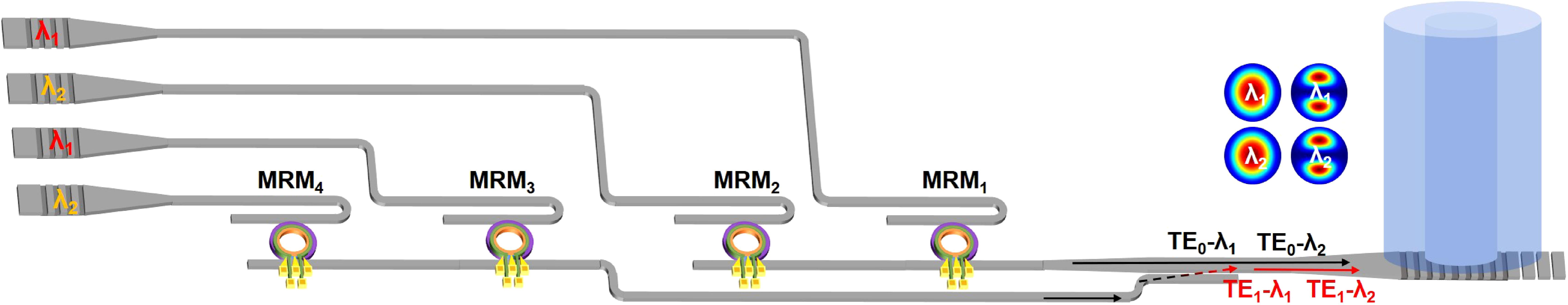
Figure 1 illustrates the schematic diagram of the proposed silicon photonic MDM-WDM transmitter. Four-channel optical signals, divided into two groups, are launched into the transmitter using an input GC array. Each group containing two wavelength channels is modulated by two add-drop MRMs sharing the same drop waveguide. With integrated TiN heaters, the resonant wavelength of each MRM can be thermally tuned to place each channel’s operating wavelength ( or ) near the resonance peak, thus effectively realizing simultaneous modulation and two-wavelength multiplexing for the two groups. The optical signals of the two groups are further combined by a tapered-asymmetric directional coupler (TADC)-based mode multiplexer, which converts one group of the modulated optical signals (two wavelength channels with and ) into the mode while the other two channels remain in the mode. Ultimately, the optical modulated signals of the four channels (represented as , , , and , respectively) are coupled into either the or the mode in the output few-mode fiber (FMF) through a dual-mode GC.
Figure 1.Schematic diagram of the proposed silicon photonic MDM-WDM transmitter.
Figure 2 displays the schematic diagram of the MRM, with a cross-sectional view of the phase shifter within the MRM. The waveguide has a width of 450 nm and a height of 220 nm with a 90 nm slab. Each MRM is fabricated with the same radius (10 µm) and gap (0.2 µm). A lateral PN junction is formed in the middle of the ring waveguide to realize high-speed electro-optic modulation based on the plasma dispersion effect. The doping concentration is for the N-type and P-type regions, and the heavily doped N-type and P-type concentrations are , located 0.5 µm away from the edge of the rib waveguide. Additionally, a TiN heater with a width of 1 µm is located 1.1 µm above the waveguide for effective thermal tuning, allowing the operating wavelengths ( and ) of the transmitter to be reconfigured with high accuracy and flexibility.
Figure 2.(a) Schematic diagram of the MRM structure. (b) Cross-sectional view of the phase shifter within the MRM.
For the proposed hybrid MDM-WDM transmitter, the dual-mode GC is of vital importance for realizing low coupling loss over the operating wavelength range. Figures 3(a) and 3(b) showcase the schematic structure of the dual-mode GC etched on a 16 µm-wide multimode waveguide. The designed parameters of the grating period, etch width, and etch depth are represented as , , and , respectively. As the effective refractive indices of the and the mode in this multimode waveguide are nearly consistent (2.8195 and 2.8183, respectively), the two modes can simultaneously achieve approximately equal diffraction efficiency in the same grating structure based on the grating equation. Additionally, a fully etched DBR structure is placed after the grating to reflect the light in forward propagation, further strengthening the upward diffraction light field. The period and etch width of the DBR structure are represented as and , respectively. Simulations of the grating and DBR structure are carried out using the Lumerical-FDTD method. With a of 571 nm, a of 680 nm, an of 285 nm, an of 180 nm, and a of 70 nm, as depicted in Fig. 3(c), both and couplings exhibit a peak coupling efficiency above 25% and a 1-dB bandwidth beyond 14 nm, effectively supporting the MDM optical fiber interface. Here, we propose the typical design of a dual-mode grating coupler fabricated via the CMOS-compatible standard process. Further enhancement of coupling efficiency could be achieved by genetic optimization[26] or an additional grating layer[27].
Figure 3.(a) Schematic diagram of the dual-mode GC. (b) Top view of the designed dual-mode GC. (c) Simulated coupling efficiency of the proposed dual-mode GC.
Based on the aforementioned design, the total integrated transmitter is fabricated via a standard silicon photonic processing provided by Compound Tek Foundry (CT), Singapore, with a top silicon layer of 220 nm and a buried oxide layer of 2 µm. The microscope images are shown in Fig. 4, occupying a total area of .
Figure 4.Microscopic images of the (a) four-channel hybrid MDM-WDM transmitter, (b) the MRM, and (c) the dual-mode GC.
The static transmission spectra of the four channels, as depicted in Figs. 5(a)–5(d), are first measured with a tunable source laser (Santec TSL-710) and a power monitor (Santec, MPM-200). The peak values of the resonance curves in Figs. 5(a) and 5(b) are used to estimate the insertion loss around 1550 nm for the and mode channels, which are approximately 10.27 and 10.67 dB, respectively. By factoring out the input fiber-waveguide grating-coupling loss calculated from the reference devices (about 4.5 dB), the coupling loss for the designed dual-mode GC is estimated to be around 6 dB for the two modes, indicating an effective coupling efficiency performance consistent with the simulation results. The transmission spectra of the and channels, as depicted in Figs. 5(c) and 5(d), are both the summation of two resonance curves, exhibiting relatively larger insertion losses with dips near the resonant peaks during static transmission measurement. This can be eliminated by thermal tuning in practical data transmission.
Figure 5.Measured static transmission spectra of the (a) TE0-λ1, (b) TE1-λ1, (c) TE0-λ2, and (d) TE1-λ2 channels.
The resonant spectra of the channel around 1550 nm under different heating voltages are presented in Fig. 6(a), indicating an extinction ratio (ER) greater than 20 dB near 1550 nm. The heating efficiency for the channel gradually increases with the voltage, reaching 246.25 pm/V at an 8-V heating voltage. The thermal tuning of the MRM for the channel also affects the transmission spectra of the channel, as it is the summation of the two micro-ring resonance curves.
Figure 6.Measured transmission spectra around 1550 nm of (a) the TE0-λ1 channel and (b) the TE0-λ2 channel with heating voltages applied to the MRM1. (c) Measured transmission spectra around 1550 nm of the TE0-λ2 channel with heating voltages applied to the MRM2. (d) Measured transmission spectra of the TE0-λ1 channel under various reverse bias voltages.
Moreover, the resonant wavelengths of the channel and channel can be staggered by applying heating voltages to either or , as depicted in Figs. 6(b) and 6(c). Therefore, effective modulation and wavelength multiplexing for these two channels can be achieved. Based on the measured transmission spectra results under various heating voltages, we select 1548.75 and 1546.8 nm as the operating wavelengths for the two mode channels, respectively, with an 8-V heating voltage applied to the of channel. Two mode channels with and exhibit a similar transmission performance (not presented in the figure due to limited space) and can also conduct modulation and multiplexing under the same operating wavelengths and heating voltage conditions as the two mode channels used. Notably, the operating wavelength channels ( and ) can be reconfigured with high accuracy and flexibility through effective thermal tuning. The resonant spectra under different reverse biases (electrical tuning) are also measured. Figure 6(d) illustrates the transmission spectra of the channel under various reverse bias voltages, with an electrical tuning efficiency of 40 pm/V at a 5-V reverse bias voltage, and the four channels show nearly equal electro-optical (EO) modulation efficiency (not presented here due to limited space).
We then characterized the frequency response of each channel through EO measurements with a 43 GHz vector network analyzer (VNA, Anritsu, MS46322B) and a 50 GHz photodetector. The measured curves are all normalized to 100 MHz. As shown in Fig. 7, the four channels exhibit similar EO responses, and a 3-dB EO bandwidth of approximately 20 GHz is obtained at the corresponding operating wavelength for each channel under a 5-V DC reverse bias. The EO bandwidth performance is mainly limited by the resistance-capacitance parameters of the doping micro-ring structure.
Figure 7.Measured EO-S21 results of the four channels under a 5-V reverse bias voltage.
To verify the high-speed performance of the proposed silicon MDM-WDM transmitter, we further set up the high-speed data transmission experiment for each channel, and the setup is shown in Fig. 8(a). A pseudo-random binary sequence (PRBS) signal is generated via an arbitrary wave generator (AWG, Keysight, M8192A) and amplified by a 55-GHz bandwidth radio frequency (RF) amplifier (SHF807C). The RF signal is combined with a 5-V reverse bias by a bias-tee and then loaded onto the lumped electrodes of each MRM through a 40-GHz RF probe (GGB, Model 40 A). The DC voltage is applied to ensure the PN junction of each MRM under a reverse-bias state. A tunable laser source (TSL-710) is utilized as the light input at the corresponding operating wavelength for each channel, with a 10 dBm output power. The laser is followed by a polarization controller (PC) to tune the polarization to the TE mode. At the output end of the transmitter, the modulated optical signal is coupled to an FMF and then amplified via an erbium-doped fiber amplifier (EDFA) to compensate for the on-chip optical insertion loss. After suppressing the amplified spontaneous emission (ASE) noise through an optical bandpass filter (BPF), the output optical signal is detected by a 50-GHz photodetector, and the corresponding photocurrent signal is finally received by a digital communication analyzer (DCA) for eye-diagram measurement or a digital storage oscilloscope (DSO) for signal sampling and off-line digital signal processing.
Figure 8.(a) Schematic diagram of the high-speed measurement setup. (b) Eye diagrams of the 32 Gbps OOK signals for the four channels on the sampling oscilloscope. (c) Measured BER curves of the 56 Gbps DMT signals for each channel. (d) Corresponding received constellations of four typical subcarriers.
Eye diagrams of the 10 to 32 Gbps on-off keying (OOK) signals for each channel are observed on the sampling oscilloscope, and Fig. 8(b) shows the measured eye diagrams of 32 Gbps OOK signals of the four channels. It can be seen that the four channels present clear open eyes with signal-to-noise ratios (SNRs) of 3.14, 3.05, 3.25, and 3.11 dB, respectively, and extinction ratios (ER) of 1.33, 1.28, 1.56, and 1.38 dB, respectively. The relatively low ER performance is mainly limited by the relatively low EO modulation efficiency and the low loaded quality factor of the MRM with the limited gain of the RF amplifier.
A higher data rate can be expected using the DMT modulation format to adapt the channel response. The 56 Gbps DMT signal is transmitted with 160 subcarriers, and the bit allocation is decided by the Fischer algorithm. Figure 8(c) illustrates the calculated bit error rate (BER) for each channel of the proposed MDM-WDM transmitter. It can be seen that all four channels exhibit a BER under a 20% forward-error-correction (FEC) threshold () with more than 1-dBm received optical power, and the corresponding received constellations of four typical subcarriers are depicted in Fig. 8(d).
4. Discussion
The proposed silicon hybrid MDM-WDM transmitter chiplet can further be utilized to achieve a 3D co-packaged transmitter optical subassembly (TOSA) via flip-chip-based electronic-photonic packaging, with the schematic diagram illustrated in Fig. 9(a). The silicon MDM-WDM transmitter chiplet is mounted on a printed circuit board (PCB), and a driver chip (Macom product: MAOM-005408) is flipped on top of the silicon MDM-WDM transmitter chiplet through Au bump-based flip-chip bonding. The differential input and output driver provided by Macom is typically with a 3-dB bandwidth of 38 GHz. As shown in Fig. 9(b), bond pads and metal lines are fabricated on the transmitter chiplet through a standard metallization process. Since the layout of the bond pads perfectly matches that of driver bumps, pin-to-pin bonding between the driver hip and the silicon photonic transmitter chiplet can be achieved. Additionally, bonding wires and metal lines are utilized for high-speed signal transmission as well as biasing and control of the driver and each channel’s MRM. The microscopic images of the 3D-packaged EPIC are shown in Figs. 9(c) and 9(d). Since the output voltage amplitude of the driver is limited to a maximum of only 1.5 V, it is difficult to effectively drive each channel’s MRM on the current silicon MDM-WDM transmitter chiplet for high-speed transmission. This problem can be addressed by future electronic-photonic co-design, thus realizing high-density, large-capacity, and energy-efficient 3D co-packaged optical interconnects through flip-chip based electronic-photonic packaging processes.
Figure 9.(a) Schematic diagram of the 3D co-packaged TOSA. (b) Schematic diagrams of the EIC and PIC. (c) Top view and (d) side view of the 3D-packaged EPIC.
In summary, we proposed and experimentally demonstrated a four-channel silicon photonic MDM-WDM transmitter chiplet, assisted with MRMs and a dual-mode GC over a footprint. The utilized add-drop MRMs can simultaneously achieve electro-optic modulation and two-wavelength multiplexing, exhibiting advantageous performance in size and power consumption. Meanwhile, the dual-mode GC with a side-distributed Bragg reflector structure achieves low coupling loss (around 6 dB) both for on-chip and modes, effectively supporting the MDM optical fiber interface. Clear open-eye diagrams of the 32 Gbps OOK signals are realized for the four channels, and a high data rate of up to signaling is also experimentally demonstrated with a BER below the 20% forward-error-correction threshold, showing potential applications for QSFP56 optical transceivers. The proposed transmitter chiplet can further be utilized to achieve a 3D co-packaged TOSA for high-density, large-capacity, and energy-efficient optical interconnects via flip-chip-based EPIC packaging.
[10] E. Timurdogan, Z. Su, R.-J. Shiue et al. 400G silicon photonics integrated circuit transceiver chipsets for CPO, OBO, and pluggable modules. Optical Fiber Communication Conference, T3H(2020).
[16] Y. Xu, J. Lin, R. Dubé-Demers et al. A single-laser flexible-grid WDM silicon photonic transmitter using microring modulators. Optical Fiber Communication Conference, W1I(2018).
[17] J. Fujikata, M. Noguchi, S.-H. Jeong et al. High-speed and 16 λ-WDM operation of Ge/Si electro-absorption modulator for C-band spectral regime. Optical Fiber Communications Conference and Exhibition (OFC), 1(2020).
[18] D. Kong, H. Xin, K. Kim et al. 300 Gb/s net-rate intra-datacenter interconnects with a silicon integrated optical frequency comb modulator. Optical Fiber Communications Conference and Exhibition (OFC), 1(2020).
Xinyi Wang, Jiangbing Du, Weihong Shen, Ke Xu, Zuyuan He, "High-density MDM-WDM silicon photonic transmitter chiplet based on MRMs and dual-mode GC for 4 × 56 Gbps 3D co-packaged optical interconnects," Chin. Opt. Lett. 22, 120001 (2024)
 AI Video Guide
  AI Picture Guide
 AI One Sentence