[1] K GEIM A, S NOVOSELOV K. The rise of graphene. Nature Materials, 6, 183-191(2007).
[2] N XIA F, H WANG, D XIAO et al. Two-dimensional material nanophotonics. Nature Photonics, 8, 899-907(2014).
[3] B OOSTINGA J, B HEERSCHE H, L LIU X et al. Gate-induced insulating state in bilayer graphene devices. Nature Materials, 7, 151-157(2008).
[4] H SEOL J, I JO, L MOORE A et al. Two-dimensional phonon transport in supported graphene. Science, 328, 213-216(2010).
[5] G LI Y, L WANG H, M XIE L et al. MoS2 nanoparticles grown on graphene: an advanced catalyst for hydrogen evolution-reaction. Journal of the American Chemical Society, 133, 7296-7299(2011).
[6] M BERNARDI, M PALUMMO, C GROSMAN J. Extraordinarysunlight absorption and one nanometer thick photovoltaics using two- dimensional monolayer materials. Nano Letters, 13, 3664-3670(2013).
[7] K PERKINS F, L FRIEDMAN A, E COBAS et al. Chemical vapor sensing with monolayer MoS2. Nano Letters, 13, 668-673(2013).
[8] S PATIL, A HARIE, S SATHAYE et al. Development of a novel method to grow mono/few-layered MoS2 films and MoS2-graphene hybrid films for supercapacitor applications. CrystEngComm, 16, 10845-10855(2014).
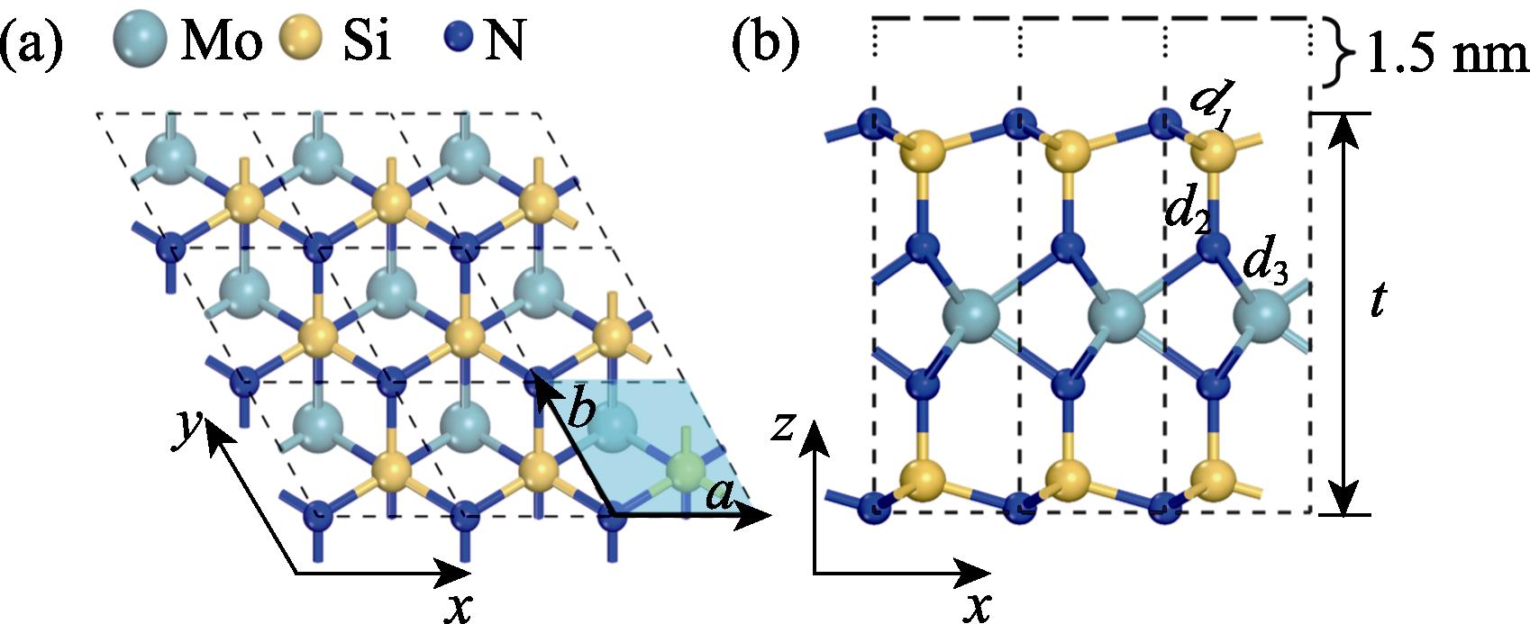
[10] L HONG Y, B LIU Z, L WANG et al. Chemical vapor deposition of layered two-dimensional MoSi2N4 materials. Science, 369, 670-674(2020).
[11] Q CAI Y, G ZHANG, W ZHANG Y. Polarity-reversed robust carrier mobility in monolayer MoS2 nanoribbons. Journal of the American Chemical Society, 136, 6269-6275(2014).
[12] A BAFEKRY, M FARAHJ, M HOAT D. MoSi2N4 sing- lelayer: a novel two-dimensional material with outstanding mechanical. thermal, electronic, optical, photocatalytic properties. Journal of Physics D: Applied Physics, 54(2021).
[13] F LI Q, X ZHOU W, G WAN X et al. Strain effects on monolayer MoSi2N4: ideal strength. Strain effects on monolayer MoSi2N4: ideal strength and failure mechanism. Physica E, 131(2021).
[14] H YU J, J ZHOU, G WAN X et al. High intrinsic lattice thermal conductivity in monolayer MoSi2N4.
[15] H ZHONG, Q XIONG W, F LÜ P et al. Strain induced semiconductor to metal transition in MA2Z4 bilayers.
[16] M CAO L, H ZHOU G, Q WANG Q et al. Two-dimensional van der waals electrical contact to monolayer MoSi2N4.
[17] D GUO S, T ZHU Y, Q MU W et al. Structure effect on intrinsic piezoelectricity in septuple-atomic-layer MSi2N4. (M = Mo and W). Computational Materials Science, 188(2021).
[18] B MORTAZAVI, B JAVVAJI, F SHOJAEI et al. Exceptional piezoelectricity. Exceptional piezoelectricity, high thermal conductivity and stiffness and promising photocatalysis in two-dimensional MoSi2N4 family confirmed by first-principles. Nano Energy, 82(2021).
[19] Y HUI Y, F LIU X, W JIE et al. Exceptional tunability of band energy in a compressively strained trilayer MoS2 sheet. ACS Nano, 7, 7126-7131(2013).
[20] G TSOUKLERI, J PARTHENIOS, K PAPAGELIS et al. Subjecting a gr-aphene monolayer to tension and compression. Small, 5, 2397-2402(2010).
[21] W PENG Z, L CHEN X, L FAN Y et al. Strain engineering of 2D semiconductors and graphene: from strain fields to band-structure tuning and photonic applications. Light: Science & Applications, 9, 190-215(2020).
[22] D VANDERBILT. Soft self-consistent pseudopotentials in a generalized eigenvalue formalism. Physical Review B, 41, 7892-7895(1990).
[23] A TKATCHENKO, A DISTASIO R, R CAR et al. Accurate. Accurate and efficient method for many-body van der waals interactions. Physical Review Letters, 108(2012).
[24] F ORTMANN, F BECHSTEDT, G SCHMIDT W et al. Semiempirical van der waals correction to the density functional description of solids and molecular structures. Physical Review B, 73, 205101(2006).
[25] D SEGALL M, P LINDAN, J PROBERT M et al. First principles simulation: ideas, illustrations and the CASTEP code. Journal of Physics: Condensed Matter, 14, 2717-2744(2002).
[26] L DONG, R NAMBURU R, T P O’REGAN et al. Theoretical study on strain-induced variations in electronic properties of monolayer MoS2. Journal of Materials Science, 49, 6762-6771(2014).
[27] C LI, W FAN B, Y LI W. Bandgap engineering of monolayer MoS2 under strain: a DFT study. Journal of the Korean Physical Society, 66, 1789-1793(2015).
[28] P MIAO Y, F MA, H HUANG Y et al. Strain effects on electronic states and lattice vibration of monolayer MoS2. Physica E: Low-dimensional Systems and Nanostructures, 71, 1-6(2015).
[29] S WU M, B XU, G LIU et al. The effect of strain on band structure of single-layer MoS2: an
[30] M LIN Q, G CUI J, X YAN et al. First-principles study on electronic structure and optical properties of single point defect graphene oxide. Journal of Inorganic Materials, 35, 1117-1122(2020).
[31] Q YU Z, H ZHANG C, D LI S. Electronic structures and optoelectronic properties of C/Ge-doped silicon nanotubes. Journal of Inorganic Materials, 30, 233-239(2015).
[32] J LI, Y LIU T, A YAO S et al. First principles study on the property of O vacancy in LuPO4 crystal. Journal of Inorganic Materials, 34, 879-884(2019).