
Huabin Wang, Yu He, Lixin Zhao. Holographic Double-Sided Photolithography Based on Improved Gerchberg-Saxton Algorithm[J]. Laser & Optoelectronics Progress, 2023, 60(16): 1609001
- Laser & Optoelectronics Progress
- Vol. 60, Issue 16, 1609001 (2023)
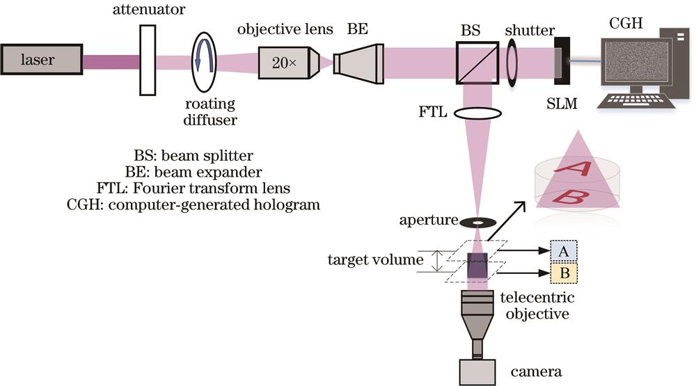
Fig. 1. Schematic of the double-sided photolithography based on computer-generated holography algorithm
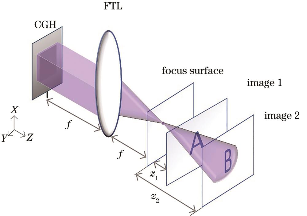
Fig. 2. Schematic of the optical path of the improved GS algorithm
Fig. 3. Flow chart of iterative optimization of improved GS algorithm
Fig. 4. Reconstructed images of light field at different depths in the target volume calculated by simulation. (a) Letter B; (b) letter A
Fig. 5. Simulated images of two-layer image plane in the presence of crosstalk. (a) Letter B; (b) letter A
Fig. 6. Diagram of experimental system of double-sided photolithography based on computer-generated holography algorithm
Fig. 7. Image plane without eliminating speckle and stray light. (a) Image plane in the presence of speckle; (b) image plane in the presence of stray light
Fig. 8. Image planes observed by the camera at different positions. (a) Image plane B; (b) image plane A
Fig. 9. Exposure results of photosensitive resin. (a) Exposure result of the front surface of the substrate; (b) exposure result of the posterior surface of the substrate
Fig. 10. Results after exposure and development of photoresist. (a) High diffraction order exposure on the front surface of the substrate;(b) zero order exposure on the posterior surface of the substrate


Set citation alerts for the article
Please enter your email address

© Copyright 2018-2021 | Chinese Laser Press. All Rights Reserved 沪ICP备15018463号-20