• Laser & Optoelectronics Progress
  • Vol. 60, Issue 17, 1714005 (2023)
Zhihui Huang1, Qike Ye2, Qijiao Ye2, and Jianhong Liao1,*
Author Affiliations
  • 1School of Information and Optoelectronic Science and Engineering, South China Normal University, Guangzhou 510006, Guangdong , China
  • 2Lijieke Laser Technology Co., Ltd., Guangzhou 511450, Guangdong , China
  • show less
    DOI: 10.3788/LOP222190 Cite this Article Set citation alerts
    Zhihui Huang, Qike Ye, Qijiao Ye, Jianhong Liao. Study on Process and Quality of Dual Laser Etching and Cleaning Flexible Copper Clad Laminate[J]. Laser & Optoelectronics Progress, 2023, 60(17): 1714005 Copy Citation Text show less
    Four stages of laser-material interaction at different power densities
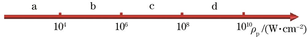
    Fig. 1. Four stages of laser-material interaction at different power densities
    Experimental scheme
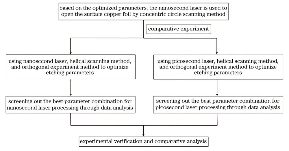
    Fig. 2. Experimental scheme
    FCCL first-order blind hole machining schematic. (a) Schematic diagram of copper foil etching by nanosecond laser concentric scanning method; (b) copper foil layer etching profile; (c) schematic diagram of spiral scanning method of etching and cleaning blind hole; (d) schematic diagram of the first-order blind hole section
    Fig. 3. FCCL first-order blind hole machining schematic. (a) Schematic diagram of copper foil etching by nanosecond laser concentric scanning method; (b) copper foil layer etching profile; (c) schematic diagram of spiral scanning method of etching and cleaning blind hole; (d) schematic diagram of the first-order blind hole section
    Laser etched copper layer morphology. (a) Radius measurement chart under optical microscope; (b) three-dimensional height map under laser confocal microscope
    Fig. 4. Laser etched copper layer morphology. (a) Radius measurement chart under optical microscope; (b) three-dimensional height map under laser confocal microscope
    Observation diagram of laser etching and cleaning blind hole. (a) Nanosecond laser etching and cleaning morphology under optical microscope; (b) picosecond laser etching and cleaning morphology under optical microscope;(c) nanosecond laser processing blind hole two-dimensional profile; (d) picosecond laser processing blind hole two-dimensional contour diagram
    Fig. 5. Observation diagram of laser etching and cleaning blind hole. (a) Nanosecond laser etching and cleaning morphology under optical microscope; (b) picosecond laser etching and cleaning morphology under optical microscope;(c) nanosecond laser processing blind hole two-dimensional profile; (d) picosecond laser processing blind hole two-dimensional contour diagram
    Optimized parameters for picosecond laser etching and cleaning of blind hole. (a) Three-dimensional color map under laser confocal microscope; (b) profile color map; (c) three-dimensional height map; (d) profile height map
    Fig. 6. Optimized parameters for picosecond laser etching and cleaning of blind hole. (a) Three-dimensional color map under laser confocal microscope; (b) profile color map; (c) three-dimensional height map; (d) profile height map
    ItemNanosecond laserPicosecond laser
    Production companyDCTDCT
    Equipment modelDirect Laser S3Direct Laser S5
    Power /W1515
    Wavelength /nm355355

    Beam type

    Pulse width /ns

    Gaussian beam

    20

    Gaussian beam

    15×10-3

    Light spot diameter /μm3025
    Table 1. Laser processing experimental equipment parameters
    LevelPower /WRepetition frequency /kHzScanning timesScanning speed /(mm·s-1
    13.0801700
    23.5902800
    34.01003900
    44.511041000
    Table 2. Factor level table
    Serial numberLevelDepth /µmRoughness of hole bottom /µm
    ABCD
    1111134.421.78
    2122234.061.67
    3133333.871.12
    4144433.021.05
    5212337.450.76
    6221435.861.20
    7234138.430.87
    8243237.860.78
    9313439.040.98
    10324339.841.03
    11331235.661.20
    12342137.640.87
    13414240.761.20
    14423139.781.23
    15432438.240.88
    16441335.021.02
    Table 3. Orthogonal experimental factor design and results
    ItemLevelPower /WRepetition frequency /kHzScanning timesScanning speed /(mm·s-1
    Depthk133.8437.9235.2437.57
    k237.4037.3936.8537.09
    k338.0536.5537.6436.55
    k438.4535.8938.0136.54
    R4.612.032.771.03
    Roughnessk11.441.181.351.19
    k20.901.301.041.21
    k31.031.051.060.99
    k41.080.931.051.03
    R0.540.370.310.23
    Table 4. Range analysis
    LevelPower /WRepetition frequency /kHzScanning timesScanning speed /(mm·s-1
    131004800
    241205900
    3514061000
    4616071100
    Table 5. Factor level table
    Serial numberLevelDepth /µmRoughness of hole bottom /µm
    ABCD
    1111135.850.57
    2122234.760.60
    3133334.520.65
    4144434.350.75
    5212336.870.47
    6221436.650.58
    7234136.480.44
    8243236.200.62
    9313437.670.23
    10324337.350.25
    11331236.750.29
    12342136.020.28
    13414238.240.28
    14423137.900.31
    15432436.260.31
    16441335.240.48
    Table 6. Orthogonal experimental factor design and results
    ItemLevelPower /WRepetition frequency /kHzScanning timesScanning speed /(mm·s-1
    Depthk134.8737.1636.5636.56
    k236.5536.6735.9836.49
    k336.9536.0036.5736.00
    k436.9135.4536.6136.23
    R2.081.710.630.56
    Optimal levelA3B1C4D1
    Roughnessk10.640.390.480.4
    k20.530.440.420.45
    k30.260.420.450.46
    k40.350.530.430.47
    R0.380.140.060.07
    Optimal levelA4B2C2D1
    Table 7. Range analysis
    ItemDepth /µmRoughness of hole bottom /µmSurface roughness /µm
    Nanosecond laser37.250.650.57
    Picosecond laser37.020.160.25
    Table 8. Optimization process etching results
    Zhihui Huang, Qike Ye, Qijiao Ye, Jianhong Liao. Study on Process and Quality of Dual Laser Etching and Cleaning Flexible Copper Clad Laminate[J]. Laser & Optoelectronics Progress, 2023, 60(17): 1714005
    Download Citation