• Laser & Optoelectronics Progress
  • Vol. 60, Issue 15, 1516002 (2023)
Dengqi Zhang1, Hanmin Tian1,2,*, Quanmin He1, Xiaoya Song1..., Wenfang Liu1 and Yuerong Wang1|Show fewer author(s)
Author Affiliations
  • 1School of Electronics and Information Engineering, Hebei University of Technology, Tianjin 300401, China
  • 2Tianjin Key Laboratory of Electronic Materials and Device, Tianjin 300401, China
  • show less
    DOI: 10.3788/LOP221606 Cite this Article Set citation alerts
    Dengqi Zhang, Hanmin Tian, Quanmin He, Xiaoya Song, Wenfang Liu, Yuerong Wang. Electronic and Optical Properties of Low-Concentration Ge Doping and Substitution of Sn and Ge for CsPbI3[J]. Laser & Optoelectronics Progress, 2023, 60(15): 1516002 Copy Citation Text show less
    Atomic structure of cubic phase perovskite
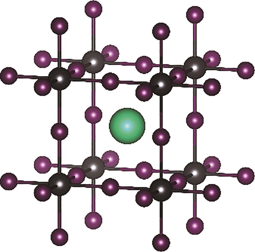
    Fig. 1. Atomic structure of cubic phase perovskite
    Total energy of system under different lattice constants based on GGA-PBE and GGA-PBEsol methods. (a) CsPbI3; (b) CsSnI3; (c) CsGeI3
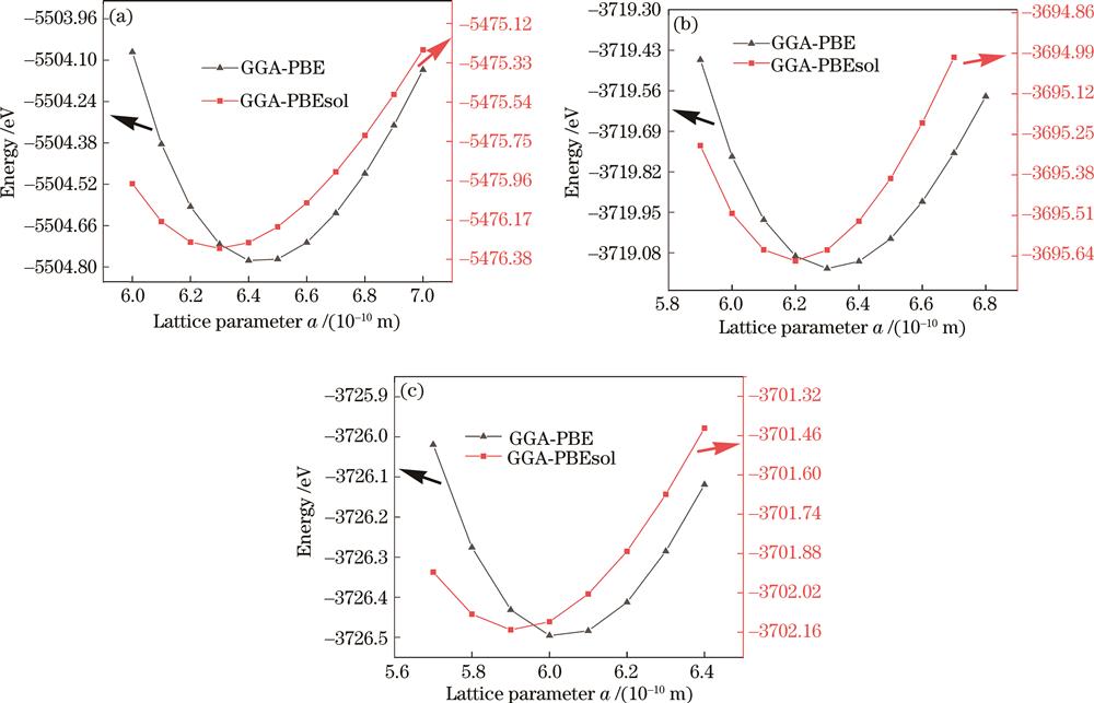
    Fig. 2. Total energy of system under different lattice constants based on GGA-PBE and GGA-PBEsol methods. (a) CsPbI3; (b) CsSnI3; (c) CsGeI3
    Calculated energy band structures based on GGA-PBE and GGA-BLYP.(a), (b) CsPbI3; (c), (d) CsSnI3; (e), (f) CsGeI3
    Fig. 3. Calculated energy band structures based on GGA-PBE and GGA-BLYP.(a), (b) CsPbI3; (c), (d) CsSnI3; (e), (f) CsGeI3
    Density of states of each material. (a) CsPbI3; (b) CsSnI3; (c) CsGeI3
    Fig. 4. Density of states of each material. (a) CsPbI3; (b) CsSnI3; (c) CsGeI3
    Calculated energy band diagram with different lattice constants of CsPbI3 with (a) a=6.0×10⁻¹⁰ m and (b) a=6.6×10⁻¹⁰ m; CsSnI3 with (c) a=6.3×10⁻¹⁰ m and (d) a=6.6×10⁻¹⁰ m; CsGeI3 with (e) a=5.8×10⁻¹⁰ m and (f) a=6.4×10⁻¹⁰ m
    Fig. 5. Calculated energy band diagram with different lattice constants of CsPbI3 with (a) a=6.0×10⁻¹⁰ m and (b) a=6.6×10⁻¹⁰ m; CsSnI3 with (c) a=6.3×10⁻¹⁰ m and (d) a=6.6×10⁻¹⁰ m; CsGeI3 with (e) a=5.8×10⁻¹⁰ m and (f) a=6.4×10⁻¹⁰ m
    Bandgap change of CsPbI3, CsSnI3, and CsGeI3 with different lattice parameters
    Fig. 6. Bandgap change of CsPbI3, CsSnI3, and CsGeI3 with different lattice parameters
    Calculated energy band and density of states of supercell CsPbI3. (a), (c) Without Ge2+ doping; (b), (d) with Ge2+ doping
    Fig. 7. Calculated energy band and density of states of supercell CsPbI3. (a), (c) Without Ge2+ doping; (b), (d) with Ge2+ doping
    Calculated optical absorption coefficients of CsPbI3, CsSnI3, and CsGeI3 at wavelength range from 200 to 1000 nm
    Fig. 8. Calculated optical absorption coefficients of CsPbI3, CsSnI3, and CsGeI3 at wavelength range from 200 to 1000 nm
    Perovskite materialCsPbI3CsSnI3CsGeI3
    GGA-PBE6.46.36.0
    GGA-PBEsol6.36.25.9
    Other work

    6.392620

    6.2621

    6.2722

    6.27623

    6.0824
    Exp.6.29256.2026
    Table 1. Lattice constants of CsPbI3, CsSnI3, and CsGeI3 based on different density functional methods
    Perovskite materialCsPbI3CsSnI3CsGeI3
    GGA-PBE1.610.450.84
    GGA-PBEsol1.5100.1700.545
    BLYP1.75000.59811.0734
    Other work

    1.4829

    1.79330

    0.73522

    0.49530

    0.9724
    Exp.1.73311.3261.332
    Table 2. Calculated bandgaps of CsPbI3, CsSnI3, and CsGeI3 based on different density functional methods
    Lattice constant /(10-10 m)Bandgap value of CsPbI3 /eVBandgap value of CsSnI3 /eVBandgap value of CsGeI3 /eV
    5.70.03400.060
    5.80.338200.1970
    5.90.615700.4383
    6.00.8666000.65417
    6.11.091100.8492
    6.21.2896101.02249
    6.31.46260.23461.1734
    6.41.61130.45451.3055
    6.51.73670.65191.4163
    6.61.839600.825861.47210
    Table 3. Bandgap values of CsPbI3, CsSnI3, and CsGeI3 with different lattice parameters
    Dengqi Zhang, Hanmin Tian, Quanmin He, Xiaoya Song, Wenfang Liu, Yuerong Wang. Electronic and Optical Properties of Low-Concentration Ge Doping and Substitution of Sn and Ge for CsPbI3[J]. Laser & Optoelectronics Progress, 2023, 60(15): 1516002
    Download Citation