
Shupei JIN, Yunong HU, Peng ZHOU, Ming LIU. Study on the electrical properties of superlattice influenced by the thickness of GaSb substrate[J]. Infrared and Laser Engineering, 2024, 53(10): 20240243
- Infrared and Laser Engineering
- Vol. 53, Issue 10, 20240243 (2024)
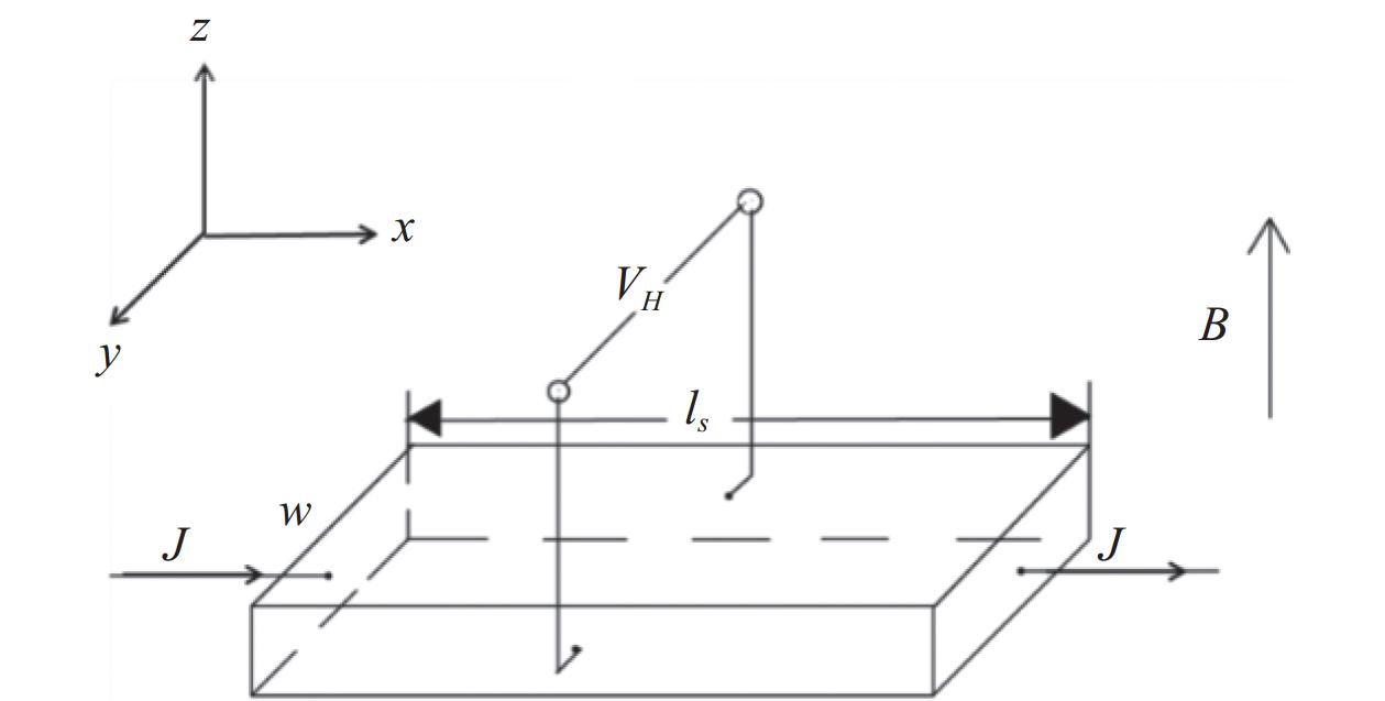
Fig. 1. Hall effect diagram

Fig. 2. Diagram of a thin film sample for Hall test
Fig. 3. Schematic diagram of the growing system of MBE
Fig. 4. Structure diagram of mechano chemical polishing
Fig. 5. Structure diagram of n doped InAs/GaSb type Ⅱ superlattice film
Fig. 6. Structure diagram of p doped InAs/GaSb type Ⅱ superlattice film
Fig. 7. (a) The electrical characteristics of n doped InAs/GaSb type Ⅱ superlattice film, it indicates that the change of carrier concentration with different thinkness of GaSb substrate; (b) The electrical characteristics of n doped InAs/GaSb type Ⅱ superlattice film, it is the change of mobility with different thinkness of GaSb substrate
Fig. 8. The electrical characteristics of p doped InAs/GaSb type Ⅱ superlattice film. (a) indicates that the change of carrier concentration with different thinkness of GaSb substrate; (b) is the change of mobility with different thinkness of GaSb substrate
|
Table 1. Hall test results of n doped InAs/GaSb type Ⅱ superlattice film with different thinkness of GaSb substrate
|
Table 2. Hall test results of p doped InAs/GaSb type Ⅱ superlattice film with different thinkness of GaSb substrate


Set citation alerts for the article
Please enter your email address

© Copyright 2018-2021 | Chinese Laser Press. All Rights Reserved 沪ICP备15018463号-20