1State Key Laboratory of Precision Spectroscopy, East China Normal University, Shanghai 200062, China
2The Extreme Optoelectromechanics Laboratory (XXL), School of Physics and Electronic Science, East China Normal University, Shanghai 200241, China
3Hefei National Laboratory, Hefei 230088, China
4State Key Laboratory of High Field Laser Physics and CAS Center for Excellence in Ultra-intense Laser Science, Shanghai Institute of Optics and Fine Mechanics (SIOM), Chinese Academy of Sciences (CAS), Shanghai 201800, China
【AIGC One Sentence Reading】:We demonstrate an on-chip Yb:TFLN Fabry-Perot laser with single-mode, narrow-linewidth, and tunable output, reaching up to 1.5 mW power.
【AIGC Short Abstract】:We demonstrate an on-chip Yb3+-doped thin-film lithium niobate Fabry–Perot microcavity laser, achieving single-frequency operation at 1030 & 1060 nm with narrow linewidth and high output power. Tuning efficiency of 4 pm/V is realized, paving the way for on-chip high-power and ultrafast lasers.
Note: This section is automatically generated by AI . The website and platform operators shall not be liable for any commercial or legal consequences arising from your use of AI generated content on this website. Please be aware of this.
Abstract
Ytterbium ion ()-doped lasers are widely used in precision machining and precision measurement fields because of their high efficiency and high power, which are primarily based on solid-state lasers and fiber lasers. Here, we demonstrate an on-chip -doped thin-film lithium niobate (Yb:TFLN) Fabry–Perot microcavity laser. We achieve single-frequency laser operation at 1030 and 1060 nm with a side-mode suppression ratio above 30 dB, an emission linewidth below 40 pm, and an output power up to 1.5 mW at 1060 nm and 0.3 mW at 1030 nm. In addition, using the electro-optic effect of lithium niobate, we achieve a laser tuning efficiency of 4 pm/V. This work opens the path to on-chip high-power and mode-locked ultrafast laser output.
1. INTRODUCTION
Owing to their simple electronic level structure (), small quantum defects, being free of self-quenching, large gain bandwidth (), long upper-state lifetimes (1–2 ms), easy high-concentration doping, and diode pumping, trivalent ytterbium () ions have been successfully used as laser-active dopants in a variety of host materials, such as crystals, glasses, and ceramics, as well as in optical fibers to generate high-power, wavelength-tunable, and mode-locked ultrafast laser outputs [1–9]. Consequently, the -doped laser has emerged as the mainstay of high-power laser systems widely utilized in both industrial and defense applications [10–12]. Typically, ytterbium lasers are based on solid-state or optical fiber systems. In the past few decades, significant progress in integrated photonics technologies has facilitated the miniaturization of table-top instruments and equipment into compact chips, resulting in substantial reductions in size, weight, power consumption, and cost [13–15]. Currently, chip-scale ytterbium lasers are based mainly on whispering gallery mode (WGM) microresonators. Although WGM lasers have extremely low thresholds, their output power is ultralow, and they often operate in multiple modes [16–18]. In contrast to WGM resonators, the Fabry–Perot (FP) cavity typically can achieve higher power and single-longitudinal-mode laser output. In addition, chip-scale ytterbium lasers have been demonstrated mainly on silica and aluminum oxide () platforms. Compared with these platforms, thin-film lithium niobate (TFLN) not only has a wide transmission window (0.35–5 μm), a low optical loss (), a relatively large refractive index ( at 1.55 μm), and a high second-order optical nonlinearity (), but also has an exceptional electro-optic coefficient () [19–22].
In this work, we combined the advantages of the FP microcavity and TFLN to realize an on-chip -doped FP cavity laser on the TFLN platform. The fabricated TFLN FP microcavity laser chip has a total footprint as compact as and generates single-frequency lasers of approximately 1030 and 1060 nm. We achieve a linewidth of 40 pm, a high power of up to 1.5 mW at 1060 nm and 0.3 mW at 1030 nm, and a side-mode suppression ratio (SMSR) larger than 30 dB. In addition, a continuous wavelength tuning of the lasing emission in the range of 50 pm at 1026.9 nm is accomplished by applying a driving voltage from to 6 V, with an EO efficiency of 4 pm/V. This work opens the path to an on-chip actively mode-locked ultrafast laser via the high gain of and high-speed phase modulation of TFLN.
2. RESULTS
A. Design and Fabrication
Reflectors are key components of the FP cavity, and on-chip Sagnac loop reflectors (SLRs) typically employ a directional coupler (DC) as a beam splitter, forming a reflector by connecting the two outputs of the DC into a circular waveguide loop. Laser emission in the 1550 nm band has been successfully demonstrated on an erbium ion ()-doped TFLN platform [23]. However, for -doped lasers aimed at generating shorter wavelengths (1030 nm or 1060 nm), mode transport through the DC necessitates a narrower coupling gap, which increases the fabrication complexity and precision requirements. Another difficulty in applying DC-based SLRs is high reflection at the laser wavelength (1030 nm or 1060 nm) and high transmission at only a slightly shorter pump wavelength (976 nm). DCs with such properties require longer coupling lengths (even of the order of centimeters), leading to larger device sizes. To achieve a small-sized laser cavity with low fabrication precision requirements, we designed an SLR based on multimode interferometer (MMI) instead of a DC for on-chip -doped laser cavities.
Sign up for Photonics Research TOC. Get the latest issue of Photonics Research delivered right to you!Sign up now
The transmission and reflectivity of the MMI-based SLR are fundamentally dependent on the coupling ratio of the MMI. The coupling ratio can be expressed as where is the input optical power and is the power coupled across the MMI.
The normalized transmission and reflectivity of the MMI-based SLR are as follows:
To achieve high transmission of the pump light and high reflection of the signal light in the MMI-based SLR, we conducted a parameter sweep simulation design. After thorough simulation and analysis, we find the optimal dimensions for the MMI, with a length of 500 μm and a width of 4.4 μm, balancing the need for efficient signal coupling with minimal pump reflection to enhance the overall performance and efficiency of the system.
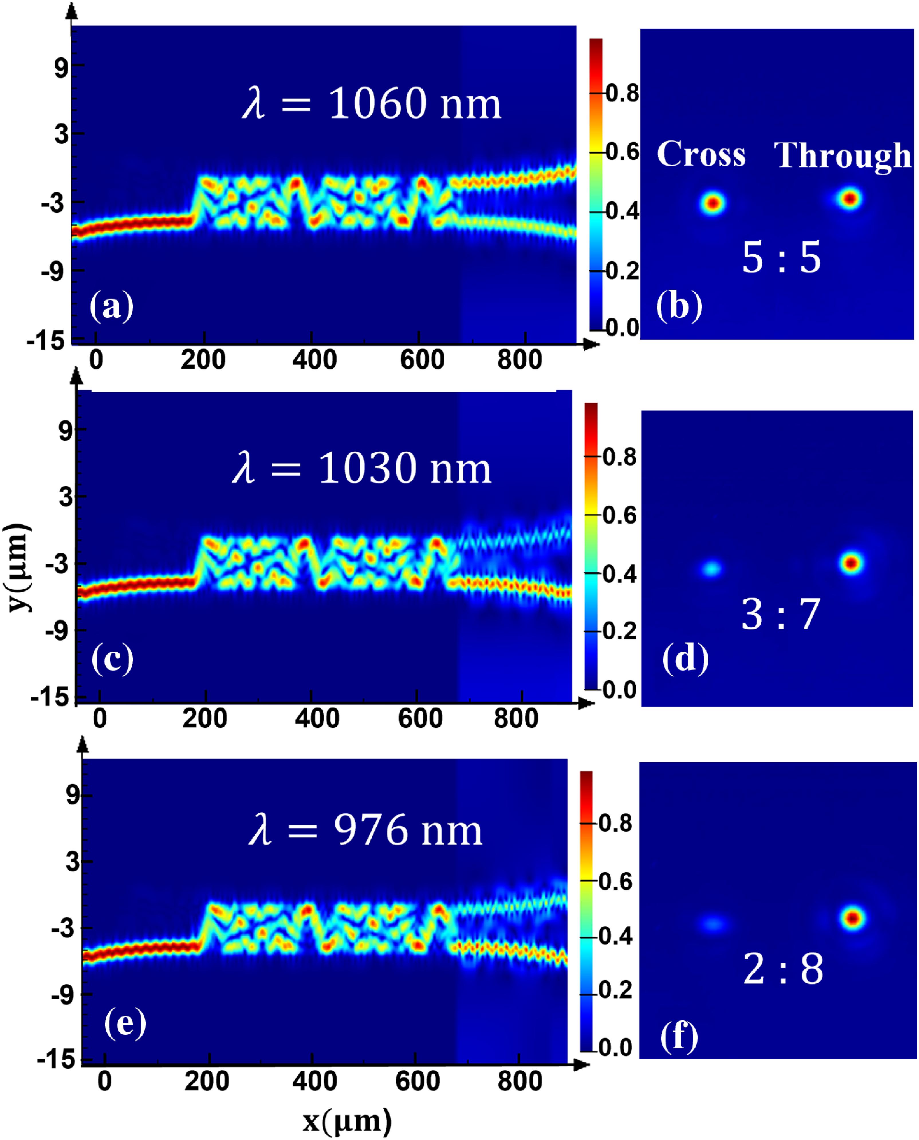
Figures 1(a), 1(c), and 1(e) show the simulated mode field distributions at 1060, 1030, and 976 nm, respectively. Figures 1(b), 1(d), and 1(f) show the experimental measurements of the cross- and through-output ports of the fabricated MMI at 1060, 1030, and 976 nm. The measured splitting ratio of the MMI is consistent with the simulation results. Additionally, owing to the low loss of the MMI itself, the input power is approximately equal to the sum of the power at the cross and through ports, so
Figure 1.Simulated mode field distributions of μμ MMIs at (a) 1060 nm, (c) 1030 nm, and (e) 976 nm, respectively. False-color infrared images generated via MATLAB at the two output ports of the actual fabricated MMI at (b) 1060 nm, (d) 1030 nm, and (f) 976 nm, respectively.
As shown in Figs. 1(b), 1(d), and 1(f), an MMI can achieve splitting ratios () of 5:5 at 1060 nm, 3:7 at 1030 nm, and 2:8 at 976 nm. By the previous Eqs. (1)–(4), we can obtain
Theoretically, this μμ-based SLR configuration can achieve 100% reflection at 1060 nm and 84% reflection at 1030 nm. However, because the signal light (1030 nm or 1060 nm) is slightly longer than the pump light (976 nm), it leads to a 64% reflection of the pump light. This partial reflection can lead to significant pump loss and a decrease in the efficiency of Yb:TFLN FP cavities.
As shown in Fig. 2, we fabricated a laser structure on a 500-nm-thick -cut -doped thin-film lithium niobate (Yb:TFLN) via photolithography assisted chemomechanical etching (PLACE) technology with a resolution of 200 nm. Further fabrication details can be found in our previous work [24,25]. The doping concentration of in the TFLN is 0.5% (mole fraction). Figure 2(a) shows a top view of the fabricated Yb:TFLN FP cavity chip, which comprises two MMI-based SLRs and a straight waveguide. It has a compact footprint of only . Each SLR has a length of 2 mm and a ring radius of 280 μm, and the ring adopts a semicircular shape connected by Bézier curves to reduce bending loss. As shown in Figs. 2(b) and 2(c), the length of the MMI is 500 μm, and its width is 4.4 μm. The straight waveguide between the two SLRs is 1.5 mm long. The top width of the ridge waveguide on the TFLN is 1 μm, and the etching depth of the ridge waveguide is approximately 250 nm. As shown in Fig. 2(a), we also integrated gold (Au) microelectrodes on the Yb:TFLN FP cavity. A pair of microelectrodes is used to load the positive and negative electrodes, and the gap between the two microelectrodes is 10 μm, as shown in Fig. 2(d).
Figure 2.(a) Optical microscope image of a Yb:TFLN FP cavity. (b) Zoomed-in optical microscope images of a complete MMI image that is 500 μm long. (c) Coupling region of the MMI with a width of 4.4 μm. (d) The gap between the two microelectrodes is 10 μm.
As shown in Fig. 3(a), the fabricated Yb:TFLN FP cavities are characterized via spectroscopic measurements of the optical transmission spectrum and laser emission. Two 976 nm pump lasers are used for bidirectional pumping through lensed fibers to couple into both sides of the Yb:TFLN FP cavities during the measurement. To enhance the stability during coupling, each lensed fiber is secured within a ceramic ferrule. Two pump/signal wavelength-division multiplexers (WDMs) are positioned at both the input and output ports of the Yb:TFLN FP cavity to measure optical transmission and lasing emission sequentially. In the absence of pumping, the left WDM is connected to a 1000–1100 nm tunable laser (CTL 1050, TOPTICA Photonics Inc.) and a 920–990 nm tunable laser (CTL 950, TOPTICA Photonics Inc.). The polarization state of the input light is adjusted via three-paddle polarization controllers (FPC561, Thorlabs Inc.). The right WDM is connected to a photodetector and an oscilloscope to characterize the quality () factor of the Yb:TFLN FP cavity near the signal and pump light. In the pumped case, the left WDM is disconnected from the signal light, whereas the right WDM is linked to an optical spectrum analyzer (OSA, AQ6374E, Yokogawa Inc.) to accurately measure the laser signal emitted by the Yb:TFLN FP cavity.
Figure 3.(a) Experimental setup used to characterize the Yb:TFLN FP cavity. The inset shows the energy level diagram of ions, the absorption and emission spectra of Yb:TFLN. (Pump, pump source; WDM, wavelength-division multiplexer; CTL, continuously tunable laser; PC, polarization controller; PD, photodetector; OSA, optical spectrum analyzer.) Normalized transmission spectra and Lorentz fitting (orange curves) around (b) 1060 nm and (c) 1030 nm for the 1030-FP laser and at (d) 976 nm for the 1060-FP laser.
As shown in the inset of Fig. 3(a), the pump and laser wavelengths correspond to the energy transitions between the ground-state manifold and the excited-state manifold of the ytterbium ion. The absorption and emission spectra of Yb:TFLN are depicted in the inset of Fig. 3(a). The absorption spectrum is measured by a Cary 5000 UV-Vis-NIR spectrophotometer, and there is strong absorption at a wavelength of 976 nm, enabling efficient pumping. The emission spectrum is measured by an FLS1000 photoluminescence spectrometer. When the excitation wavelength is set at 910 nm, there are relatively strong emission peaks at 1030 and 1060 nm, resulting in a high gain. As shown in Figs. 3(b) and 3(c), the factors of the FP cavity are determined to be and , respectively, at wavelengths of 1030 nm and 1060 nm by employing Lorentz fitting (orange curves). The mode wavelength interval, observed between two adjacent peaks in the normalized transmission, corresponds to the free spectral range (FSR) of the Yb:TFLN FP cavities, which is measured to be close to 27 pm for both cavities. Furthermore, as shown in Fig. 3(d), a factor of at 976 nm is measured for the Yb:TFLN FP cavity, suggesting that the pump light resonates within the cavity as well. The high reflectivity of the 976 nm (64% as mentioned before) wavelength by the MMI-based SLR is attributed to the broad bandwidth of the MMI, which facilitates this resonance. This phenomenon underscores the intricate interplay between the MMI design and the resonator’s spectral behavior, highlighting the importance of careful engineering in achieving optimal performance.
As shown in Fig. 4(a), the spectral signal of the FP cavity laser is captured by the OSA across a broad sweep range spanning 100 nm. The spectral purity, governed by mode-dependent loss and gain competition, is evidenced by a predominant single-mode signal with an SMSR of approximately 30 dB within the 1000–1100 nm wavelength range. Figure 4(b) presents a detailed view of the lasing emission spectrum, featuring a linewidth of 40 pm at 1029.6 nm. Importantly, the linewidth is constrained by the resolution of the OSA used in our experiment, which is approximately 20 pm. Furthermore, Fig. 4(c) illustrates the relationship between the on-chip output power of the FP cavity laser and the input pump power. The lasing threshold is measured to be approximately 6.48 mW via linear fitting. As the pump power increases, a corresponding increase in the on-chip output power of the Yb:TFLN FP cavity laser is observed. The slope efficiency for the FP cavity laser is relatively low at 0.56%, which is attributed primarily to the substantial reflection of the pump power by the MMI-based SLR prior to its entry into the resonant cavity. As shown in Fig. 4(b), we measure a maximum output power of 0.3 mW for laser operation at a wavelength of 1029.6 nm when the pump power input into the resonator is 52.4 mW. The coupling efficiency between the waveguide and lensed fiber is 9 dB at a wavelength of 1030 nm.
Figure 4.Lasing characterization of the Yb:TFLN FP cavity under a bidirectional pump with two 976 nm pump lasers. (a) Output optical spectrum of the 1030-FP laser from 1000 to 1100 nm. (b) Enlarged spectrum around a wavelength of 1029.6 nm; the lasing peak is fitted with a Lorentzian line shape (orange); the inset shows an infrared image of the mode-field distribution at 1030 nm. (c) On-chip laser power of the 1030-FP laser versus the input pump power. (d) Output optical spectral signal over a wide sweep of 100 nm of the 1060-FP laser. (e) Spectral amplification near 1062.6 nm; the inset shows an infrared image of the output port of the 1060-FP laser at 1060 nm. (f) Plot of the on-chip output power versus the input pump power of the 1060-FP laser.
We successfully generated a single-mode laser at 1060 nm by reducing the thickness of the MMI by 15 nm. To reduce the thickness of MMI is to change the mode propagation constant and phase difference between modes. The interference patterns of the modes under this MMI have less loss at 1060 nm, which optimizes the reflection conditions of 1060 nm light to achieve a single wavelength output. As shown in Fig. 4(d), we also performed corresponding measurements for the FP cavity laser, yielding a single-longitudinal mode spectrum output with an SMSR of approximately 33 dB across a 100 nm wavelength span, as characterized by the OSA. This laser has a linewidth of 53 pm and achieves a maximum output power of 1.5 mW at a wavelength of 1062.6 nm with a pump power of 45.4 mW [Fig. 4(e)]. We measure a lasing threshold of 18.13 mW and a slope efficiency of 4.61% for the FP cavity laser, and the output waveguide of this FP cavity has a coupling loss of 8 dB to the lensed fiber at 1060 nm.
The mode of the output lasing corresponding to the signal light wavelengths is visualized via an objective together with an infrared camera (InGaAs Camera C12741-03, Hamamatsu Photonics Co., Ltd.). As shown in the insets of Figs. 4(b) and 4(e), the captured infrared images are subsequently processed via MATLAB to generate false-color images for clearer visualization, and the lasing is in the fundamental spatial mode. Therefore, the Yb:TFLN FP cavity laser operates in not only single-longitudinal mode but also single-transverse mode at 1030 and 1060 nm.
Finally, we integrated a pair of microelectrodes on the Yb:TFLN FP cavity laser to obtain a continuously tunable laser. We fabricated 30 nm Cr/500 nm Au microelectrodes on a Yb:TFLN FP cavity laser via the PLACE technique; more fabrication details of the microelectrodes can be found in our previous work [26]. Au has high electrical conductivity because of its weak bonding with TFLN, and a layer of Cr film is bonded at the bottom between the TFLN layer and the Au film. As shown in Figs. 2(a) and 2(d), the length of the microelectrodes near the straight waveguide is approximately 1 mm, and the gap between them is 10 μm. Figure 5 shows the wavelength tunability with applied voltages through the microelectrodes. The inset of Fig. 5(a) shows a pair of probes used to connect the microelectrodes and the DC power supply. Figure 5(a) depicts the normalized laser output under different voltage loads on the microelectrode. The laser output wavelength inevitably experiences mode hopping with increasing voltage, so only the laser wavelengths at , 0 V, , and are shown. A linear relationship was observed between the difference in the laser wavelength and the applied voltage, as shown in Fig. 5(b). As the applied voltage increased from to 6 V, the laser wavelength increased by approximately 50 pm at approximately 1026.9 nm and the EO tuning efficiency was approximately 4 pm/V. We also found that mode hopping occurs when the applied voltage exceeds 6 V.
Figure 5.Wavelength tunability with applied voltages through microelectrodes. (a) Normalized laser output at voltages of , 0 V, , and ; the inset shows the probes used to connect the microelectrodes and DC power supply. (b) Linear relationship between the difference in wavelength and voltage applied to the electrodes.
In conclusion, we designed and fabricated an on-chip FP microcavity laser on a Yb:TFLN platform with a footprint of . This Yb:TFLN FP cavity demonstrated high power, narrow linewidth, and single-mode lasing emission at both 1030 and 1060 nm under bidirectional pumping at 976 nm. These results underscore the potential of the Yb:TFLN FP cavity for high-performance photonic applications. Owing to the broad bandwidth of the MMI, the MMI-based SLR reflects a portion of the pump power while reflecting the signal light. This results in suboptimal utilization of the pump light, thereby affecting the overall efficiency of the system. To address this limitation, future work will focus on enhancing pump light utilization through innovative pumping methods and structural optimizations of the device to obtain a higher lasing output. We will also design and fabricate a spot-size converter to improve the coupling efficiency between fibers and the Yb:TFLN FP cavity laser chip for higher power output.
 AI Video Guide
  AI Picture Guide
 AI One Sentence