• Advanced Photonics Nexus
  • Vol. 2, Issue 5, 056003 (2023)
Zhiyong Wu1,2 and Zhengji Xu1,2,*
Author Affiliations
  • 1Sun Yat-sen University, School of Microelectronics Science and Technology, Zhuhai, China
  • 2Sun Yat-sen University, Guangdong Provincial Key Laboratory of Optoelectronic Information Processing Chips and Systems, Zhuhai, China
  • show less
    DOI: 10.1117/1.APN.2.5.056003 Cite this Article Set citation alerts
    Zhiyong Wu, Zhengji Xu, "Achromatic on-chip focusing of graphene plasmons for spatial inversions of broadband digital optical signals," Adv. Photon. Nexus 2, 056003 (2023) Copy Citation Text show less
    Achromatic on-chip focusing lenses and mode properties of the AGPPs propagating within a single unit cell of the GIWAL. (a) Schematic structure of the coupling grating and the GIWAL. (b) Cross section of the GIWAL and Cartesian coordinate system employed. Dependences of (c) the effective refractive index and (d) the propagation length of the AGPPs on the width of the dielectric strip for different frequencies of the incident lights. The solid and dashed curves represent analytic results, and the circles, triangles, and squares on the corresponding curves represent numerical simulations. The inset in (c) represents the cross section of a single unit cell of the GIWAL.
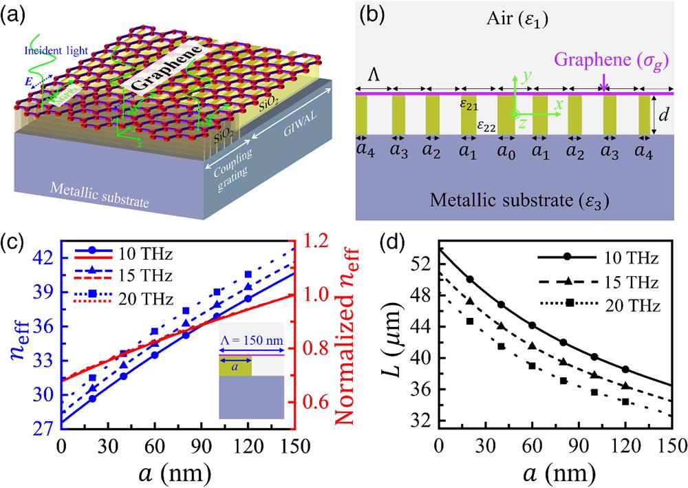
    Fig. 1. Achromatic on-chip focusing lenses and mode properties of the AGPPs propagating within a single unit cell of the GIWAL. (a) Schematic structure of the coupling grating and the GIWAL. (b) Cross section of the GIWAL and Cartesian coordinate system employed. Dependences of (c) the effective refractive index and (d) the propagation length of the AGPPs on the width of the dielectric strip for different frequencies of the incident lights. The solid and dashed curves represent analytic results, and the circles, triangles, and squares on the corresponding curves represent numerical simulations. The inset in (c) represents the cross section of a single unit cell of the GIWAL.
    On-chip focusing and optical pendulum effects of the AGPPs in the GIWAL and mode properties of the AGPPs supported by the entire GIWAL. (a) Refractive index profile and (b) the propagation constant of the waveguide modes for Mikaelian lens (red), precise GIWAL (green), and stepped GIWAL (blue), respectively. (c) Normalized electric field |E|2 of the 0th, 1st, 2nd, and 9th order AGPP modes on the cross section of the stepped GIWAL. The purple line, the gray box, and the area between them indicate the locations of graphene, metallic substrate, and SiO2 grating, respectively. (d) Both the trajectories of rays and the refractive index profile on the y=0 plane in Mikaelian lens. Evolutions of the normalized electric field |E|2 of the AGPPs on the y=0 plane in the stepped GIWAL for (e), (f) numerical simulations with losses and analytical results (g), (h) without losses and (i), (j) with losses, respectively. The broad arrows in (e), (g), and (i) represent the incident lights coupled to the AGPPs through the extended coupling grating, whereas the narrow arrows in (f), (h), and (j) represent the incident lights coupled to the AGPPs through the local coupling grating. The frequency of the incident light is f=15 THz, and the focal length of the on-chip focusing is fL=10 μm.
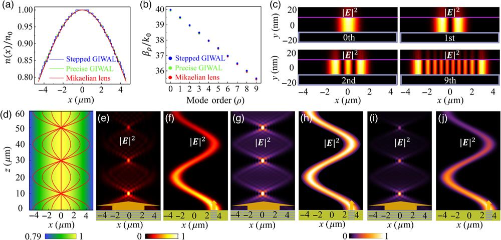
    Fig. 2. On-chip focusing and optical pendulum effects of the AGPPs in the GIWAL and mode properties of the AGPPs supported by the entire GIWAL. (a) Refractive index profile and (b) the propagation constant of the waveguide modes for Mikaelian lens (red), precise GIWAL (green), and stepped GIWAL (blue), respectively. (c) Normalized electric field |E|2 of the 0th, 1st, 2nd, and 9th order AGPP modes on the cross section of the stepped GIWAL. The purple line, the gray box, and the area between them indicate the locations of graphene, metallic substrate, and SiO2 grating, respectively. (d) Both the trajectories of rays and the refractive index profile on the y=0 plane in Mikaelian lens. Evolutions of the normalized electric field |E|2 of the AGPPs on the y=0 plane in the stepped GIWAL for (e), (f) numerical simulations with losses and analytical results (g), (h) without losses and (i), (j) with losses, respectively. The broad arrows in (e), (g), and (i) represent the incident lights coupled to the AGPPs through the extended coupling grating, whereas the narrow arrows in (f), (h), and (j) represent the incident lights coupled to the AGPPs through the local coupling grating. The frequency of the incident light is f=15  THz, and the focal length of the on-chip focusing is fL=10  μm.
    Achromatic on-chip focusing of the AGPPs in the GIWAL. (a) Normalized electric field |E|2 of the AGPPs propagating along the z-direction on the y=0 plane in the stepped GIWAL for incident frequencies of 10 THz (lower panel), 15 THz (middle panel), and 20 THz (upper panel), respectively. (b) Refractive index profiles of the stepped GIWAL for incident frequencies of 10 THz (red), 15 THz (blue), and 20 THz (green), respectively. The focal length of the on-chip focusing is fL=10 μm.
    Fig. 3. Achromatic on-chip focusing of the AGPPs in the GIWAL. (a) Normalized electric field |E|2 of the AGPPs propagating along the z-direction on the y=0 plane in the stepped GIWAL for incident frequencies of 10 THz (lower panel), 15 THz (middle panel), and 20 THz (upper panel), respectively. (b) Refractive index profiles of the stepped GIWAL for incident frequencies of 10 THz (red), 15 THz (blue), and 20 THz (green), respectively. The focal length of the on-chip focusing is fL=10  μm.
    Spatial inverter for broadband digital optical signals based on the achromatic GIWAL. Normalized electric field |E|2 of the AGPPs propagating along the z direction on the y=0 plane in the GIWAL for incident frequencies of (a) 10 THz, (c) 15 THz, and (e) 20 THz, respectively. The digital optical signals at the input end of the GIWAL are (a) “10001000100010001000,” (c) “11001100110011001100,” and (e) “11101110111011101110,” respectively. Digital encoding of the input signal on the line of z=0 (input end, blue) and the normalized electric field |E|2 of the AGPPs on the line of z=2fL (output end, orange) for incident frequencies of (b) 10 THz, (d) 15 THz, and (f) 20 THz, respectively. The black curve is the digital encoding of the output signal. The focal length of the on-chip focusing is fL=10 μm.
    Fig. 4. Spatial inverter for broadband digital optical signals based on the achromatic GIWAL. Normalized electric field |E|2 of the AGPPs propagating along the z direction on the y=0 plane in the GIWAL for incident frequencies of (a) 10 THz, (c) 15 THz, and (e) 20 THz, respectively. The digital optical signals at the input end of the GIWAL are (a) “10001000100010001000,” (c) “11001100110011001100,” and (e) “11101110111011101110,” respectively. Digital encoding of the input signal on the line of z=0 (input end, blue) and the normalized electric field |E|2 of the AGPPs on the line of z=2fL (output end, orange) for incident frequencies of (b) 10 THz, (d) 15 THz, and (f) 20 THz, respectively. The black curve is the digital encoding of the output signal. The focal length of the on-chip focusing is fL=10  μm.
    Zhiyong Wu, Zhengji Xu, "Achromatic on-chip focusing of graphene plasmons for spatial inversions of broadband digital optical signals," Adv. Photon. Nexus 2, 056003 (2023)
    Download Citation