• Chinese Optics Letters
  • Vol. 22, Issue 10, 103601 (2024)
Tianlun Jin1, Chenxu Zhu2, Yang Qiu1, Xingyan Zhao1..., Qize Zhong1, Yuan Dong1,3, Qinghua Song4, Bo Cui2, Shaonan Zheng1,3,* and Ting Hu1|Show fewer author(s)
Author Affiliations
  • 1School of Microelectronics, Shanghai University, Shanghai 201800, China
  • 2Department of Electrical and Computer Engineering, University of Waterloo, Waterloo, Ontario N2L 3G1, Canada
  • 3Shanghai Collaborative Innovation Center of Intelligent Sensing Chip Technology, Shanghai University, Shanghai 201800, China
  • 4Tsinghua Shenzhen International Graduate School, Tsinghua University, Shenzhen 5l8055, China
  • show less
    DOI: 10.3788/COL202422.103601 Cite this Article Set citation alerts
    Tianlun Jin, Chenxu Zhu, Yang Qiu, Xingyan Zhao, Qize Zhong, Yuan Dong, Qinghua Song, Bo Cui, Shaonan Zheng, Ting Hu, "Metasurface-driven dots projection based on generalized Rayleigh-Sommerfeld diffraction theory," Chin. Opt. Lett. 22, 103601 (2024) Copy Citation Text show less

    Abstract

    The diffractive optical element (DOE) is an important component of three-dimensional (3D) imaging systems based on structured light. In this work, we designed the metasurface-driven DOEs based on generalized Rayleigh–Sommerfeld diffraction theory to project large field of view (FOV) pseudo-random dot array for 3D imaging. We measured an efficiency of 61.04% and root-mean-square error (RMSE) of 0.45 for the 60° FOV sample and an efficiency of 42.96% and RMSE of 0.75 for the 144° FOV sample. Because the pattern is designed based on the generalized Rayleigh–Sommerfeld diffraction theory, the projected pattern is similar to the target pattern and has even intensity.

    1. Introduction

    With the development of computer and Internet technology, cameras and image sensors have increasingly higher requirements for three-dimensional (3D) imaging that contain depth information[1]. 3D imaging solutions typically use time-of-flight (ToF) and structured light technique[2,3]. The structured light is widely used in motion perception and face recognition because of its high spatial resolution for short distance ranging[4]. The generation of structured light mainly depends on the diffractive optical element (DOE)[5]. The surface of traditional DOE is etched into different depths to form different phases. Dammann grating is a typical binary-phase DOE[6,7]. However, Dammann grating has the problems of low efficiency and small field of view (FOV) angle because of its binary phase modulation and large pixels[8,9]. Multiple phase levels, equivalent to multiple etching depths, are essential to improve efficiency of Dammann grating. However, multiple etching depths usually increase the complexity of fabrication. Meanwhile, large pixels lead to poor performance in a large FOV, including the uniformity and low efficiency of the generated beam[10].

    A metasurface is a kind of artificial ultrathin planar optical nanostructure[1113] that has been widely used in recent years to control the polarization[14,15], phase, and amplitude of incident light on the subwavelength scale[1618]. A variety of applications can be realized for better performance by using a metasurface, including color filters[19,20], holographic displays[21,22], beam shapers[23], and beam steering[23,24]. The metasurface can modulate the phase of incident light at subwavelength scale, solving the large pixel problem of traditional DOE and effectively improving diffraction efficiency at a large FOV. By using various nanopillar structure sizes instead of multiple etching depths, metasurfaces can achieve multiple phase level modulation without complex fabrication.

    In recent years, some works on using metasurfaces to generate structured light have been reported. Li et al. produced wafer-level metasurfaces based on 12-inch immersion lithography technology, proving the feasibility of large-scale production based on metasurface point projection[25]; Wang et al. demonstrated that DOE-based metasurfaces can also be highly integrated with on-chip light sources, opening new perspectives for the design of structured light systems with compactness, light weight, and scalability[2628]. Many structured light projections have been proposed. Zhang et al. designed a dot array based on vector diffraction theory with high overall diffusion efficiency and low efficiency error of target orders[29], which can be used as a beam splitting device. Ni et al. also designed the structured light projection based on vector diffraction theory[30], which can achieve an FOV angle of 120° with an efficiency of 59.1%. However, the first two devices have a limited number of diffraction orders and the area covered by the dot array is too small to be applied to depth perception. Using fast Fourier transform (FFT), designed structured light projection can generate more points. Kim et al. made a structured light projection with an FOV angle approaching 180°[31], resulting in a dot array of about 10,000 dots covering the entire transmitted space. Hsu et al. made a system to project approximately 45,700 infrared (IR) dots from a compact 297-µm-dimention metasurface[32]. Jing et al. used a structured light projection with 1201 points to reconstruct 3D information[33]. However, a large FOV structured light projection designed using the Fresnel approximate diffraction algorithm, which only uses FFT to calculate far-field patterns, has the problems of pattern distortion and uneven intensity due to violation of the paraxial approximation.

    In this paper, we try to overcome the problems that occur when designing large FOV structured light projection with FFT. We use the Rayleigh–Sommerfeld (R-S) integral instead of FFT to calculate the far-field diffraction of light to optimize the typical Gerchberg–Saxton (G-S) algorithm. We present the demonstration of two metasurface-based structured light projections that project dot arrays with two FOV angles of 60° and 144°, operating at near-infrared 940 nm suitable for 3D imaging. The polarization-independent metasurface consists of a silicon cylinder on a fused silica substrate. We use the optimized G-S algorithm to calculate the phase distribution of a single supercell. Then, the supercells are periodically arranged along the x and y directions, forming the whole metasurface. On the basis of regular dot array, we encode the dots to generate a pseudo-random pattern, which can improve the anti-interference ability. We experimentally measured structured light projections with an efficiency of 61.04% and 42.96% with a root-mean-square error (RMSE) of 0.45 and 0.75 in a 60° FOV sample and a 144° FOV sample, respectively.

    2. Theory

    We use the diffraction effect of a single scatterer and the interference effect caused by the periodic arrangement of scatterers to generate a dot array[3436]. According to the Huygens effect, each position in the wavefront can be considered as a point wave source that generates spherical secondary waves, and every subsequent wavefront can be considered as the envelope of these secondary waves. If the interaction between each unit cell is not considered, the light source passing through a metasurface composed of n×n unit cells will form n×n sub-wave sources. By designing the unit cells that make up the metasurface, each sub-wave source has the appropriate phase and amplitude to form the desired diffraction pattern. Considering the application field of structured light, we choose near-infrared, which is invisible to the human eye, as the working wavelength. In the near-infrared range, the vertical cavity surface-emitting laser (VCSEL) technology near 940 nm is relatively mature. So, the metasurface is designed for the wavelength of 940 nm; we choose amorphous Si (a-Si) as the material of the cylinder and silicon dioxide (SiO2) as the material of the substrate, as shown in Fig. 1(a). Figure 1(b) shows the top view of the partial metasurface. The height H of the unit cell is fixed at 820 nm, and the period P is fixed at 460 nm. Using the finite-difference time-domain (FDTD) method, we simulate the relationship between the radius R of the unit cell and the transmission phase difference of light passing through the unit cell, as shown in Fig. 1(c).

    (a) Illustration of a metasurface composed of silicon nanometer cylinders and fused silica substrate; (b) top view of the metasurface; (c) diagram of transmission and phase difference variation with radius of unit cell.

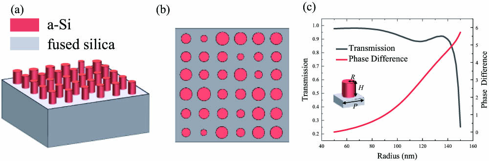
    Figure 1.(a) Illustration of a metasurface composed of silicon nanometer cylinders and fused silica substrate; (b) top view of the metasurface; (c) diagram of transmission and phase difference variation with radius of unit cell.

    By using an iterative discrete 2D Fourier transform, i.e., the G-S algorithm, the phase required to generate the target diffraction pattern can be calculated. The far-field diffraction pattern used for calculating light in typical G-S algorithms can be represented by the following equation: Uo(xo,yo)=1jλzexp(jkz)Ui(xi,yi)×exp{jk2z[(xoxi)2+(yoyi)2]}dxidyi.

    In Eq. (1), k=2π/λ is the number of waves in free space (λ is the light wavelength), and z is the diffraction distance. Uo and Ui are the electric field distributions on the imaging plane and on the metasurface plane, respectively. (xo,yo) and (xi,yi) are the corresponding coordinates. However, paraxial approximation is made when FFT is used for calculation, making it only applicable for small FOV angles calculations. For large FOV angles calculation, it may cause significant errors, including pattern distortion and uneven intensity[10]. Therefore, we have made some optimization, using R-S diffraction instead of FFT to calculate the electric field distribution on the imaging plane, as shown in Fig. 2(a). R-S diffraction integral can be expressed as Uo(xo,yo)=eikriλzz2r2Ui(xi,yi)×ei2zdz(xixozr+yiyozr)dxidyi,where r is the distance between sample points on the imaging plane and the metasurface plane, r=(xoxi)2+(yoyi)2+z2.

    (a) Flowcharts of typical G-S algorithm and optimized G-S algorithm; (b), (c) implementation principles of regular dot array and pseudo-random dot array; (d) target light intensity distribution at a distance of 0.5 m; (e), (f) simulated diagrams of normalized light intensity distribution at a distance of 0.5 m generated by the structured light projections based on FFT and generalized R-S diffraction theory.

    Figure 2.(a) Flowcharts of typical G-S algorithm and optimized G-S algorithm; (b), (c) implementation principles of regular dot array and pseudo-random dot array; (d) target light intensity distribution at a distance of 0.5 m; (e), (f) simulated diagrams of normalized light intensity distribution at a distance of 0.5 m generated by the structured light projections based on FFT and generalized R-S diffraction theory.

    Equation (2) can be used to solve the diffraction problems at large angles because no paraxial approximation is performed. Compared to calculations using FFT, Eq. (2) can be more accurate[37]. We obtain the phase required to generate far-field diffraction patterns by using the optimized G-S algorithm. The layout of the supercell, including 101×101 unit cells, is generated by placing the unit cell in corresponding transmission phase. We make periodic arrangement of the designed supercells in the x and y directions, which is described by a 2D Dirac comb function. The far-field pattern is the product of the supercell diffraction effect and the 2D Dirac comb function after the Fourier transform. By designing the target diffraction pattern of a single supercell, each dot in the regular dot array can be encoded to produce a pseudo-random dot array, as shown in Figs. 2(b) and 2(c).

    To verify the effectiveness of the R-S diffraction theory, we simulated two structured light projections for the same target pattern based on different theories. The target pattern is a square with a length and width of 0.8 m at a distance of 0.5 m from the metasurface. Figures 2(e) and 2(f) show simulated diagrams of the normalized light intensity distribution at a distance of 0.5 m generated by the structured light projections based on FFT (pattern A) and generalized R-S diffraction theory (pattern B), respectively. It can be clearly seen that pattern A has significant shape distortion, more like a cross. Pattern B is more like a square, with only a slight deformation at the four corners of the square. The reason for the slight deformation in the results may be that the selected metasurface units do not match the calculated phase well, as the phase corresponding to the metasurface units is simulated by a single unit in periodic boundary conditions. A single metasurface unit placed within the entire metasurface device may not satisfy its periodic boundary conditions, resulting in slight deformation. We take the light intensity from 0.4m to 0.4 m in the x direction and y direction as the target region, for efficiency and uniformity analysis. The efficiency and uniformity of pattern A are 44% and 0.78, the efficiency and uniformity of pattern B are 53% and 0.66, where efficiency is defined as the ratio of the sum of intensities in the target region to the sum of intensities across the entire region. Uniformity is defined as 1Imean1Mi=1M(IiImean)2.

    Here, M is the total number of points used for calculation, Ii is the ith intensity, and Imean is the average intensity in target region.

    We also conducted an experimental comparison on the improvement of distortion between R-S diffraction and the FFT algorithm. We designed a square with a diffraction angle of 30°. In order to obtain a full view of the projection pattern, we first photographed the far-field pattern on the side at a distance of 6.5 cm, as shown in Figs. 3(a) and 3(b). Figure 3(a) is designed by FFT and Fig. 3(b) is designed by R-S diffraction. We reduced the impact of zeroth order diffraction on photo shooting by making a hole in the screen to allow zeroth-order diffraction to pass through. In order to make the edges of the square clear enough, we adjusted the exposure time of the camera, so we did not calculate the efficiency of these two images. We judge the distortion situation by the angle of the square in the far-field pattern. We shot one corner of the square from the front, as shown in Figs. 3(c) and 3(d). The angle of the square designed by FFT and R-S theory methods θ1 is 60° and 84°, respectively. The target angle of the square θ0 is 90°, and distortion is defined as 1θ1/θ0. The distortion of DOE designed by FFT and R-S theory is 33.3% and 6.7%, respectively. Compared to the FFT method, the structured light projection based on the R-S diffraction theory shows improved shape, higher efficiency, and more uniform intensity.

    (a), (b) Experimental diagrams of light intensity distribution at a distance of 6.5 cm generated by the structured light projections based on FFT and generalized R-S diffraction theory, separately; (c), (d) experimental diagrams of enlarged view of square corner based on FFT and generalized R-S diffraction theory, separately.

    Figure 3.(a), (b) Experimental diagrams of light intensity distribution at a distance of 6.5 cm generated by the structured light projections based on FFT and generalized R-S diffraction theory, separately; (c), (d) experimental diagrams of enlarged view of square corner based on FFT and generalized R-S diffraction theory, separately.

    3. Fabrication

    The fabrication process is shown in Fig. 4(a). We grew an 820-nm-thick a-Si thin film on a 500 µm fused silica substrate using plasma-enhanced chemical vapor deposition (PECVD). Subsequently, a resist layer was spin-coated on the a-Si film. After electron beam lithography (EBL), the resist was removed and the patterns were transferred to the 20-nm-thick chromium (Cr) as a hard mask layer. With a mixture of C4F8 and SF6, we used inductively coupled plasma-reactive ion etching (ICP-RIE) to etch a-Si layer to form a-Si nanopillars. After etching the sample, we removed the hard mask and obtained the final structure. The scanning electron microscopy (SEM) images of the samples are shown in Figs. 4(b) and 4(c). The height of the unit cell is fixed at 820 nm, with a diameter range of 100 to 300 nm; the maximum aspect ratio is 8.2, and the minimum gap is 120 nm.

    (a) Schematic illustration of fabrication process; (b) top view SEM image of the metasurface; (c) tilted-view SEM image of the metasurface.

    Figure 4.(a) Schematic illustration of fabrication process; (b) top view SEM image of the metasurface; (c) tilted-view SEM image of the metasurface.

    4. Result

    We evaluate the device using efficiency and RMSE. Efficiency is defined as the sum of the intensities converted into spots normalized to the intensity of the incident laser. RMSE is defined as 11/N1Ni=1N(Ii1N)2,where N is the total number of designed spots, and i is the ith-order diffraction intensity. N=360 for the 60° FOV sample and N=600 for the 144° FOV sample. Vectorial electromagnetic calculation, executed by the commercial software Lumerical-FDTD solutions (Lumerical Solutions, Vancouver, Canada), is utilized to simulate the structures. We obtain an efficiency of 64.9% and 37.2% with an RMSE of 0.27 and 0.46 in a single supercell of the 60° FOV sample and the 144° FOV sample, respectively. For experimental measurement of intensity of diffracted beams, we set up an experimental apparatus shown in Fig. 5(a) to test the metasurface sample. The 940 nm laser (LD-PD PL-NL-940-A-A81-PA) is collimated through a collimator, and then an aperture is used to limit the spot size of the incident light. An IR camera (Allied Vision Goldeye G-030 TEC1) is used to capture diffraction patterns projected onto a paper screen. The diffraction patterns of light transmitted through the metasurfaces projected onto the paper screen are shown in Figs. 5(b) and 5(d). Figures 5(c) and 5(e) are the target diagrams of the metasurfaces. Because the near-infrared camera used for shooting is not on the optical axis, we performed a simple stretching process on Fig. 4(b) to make the projection range circular. We measured an efficiency of 61.04% and an RMSE of 0.45 for the 60° FOV sample and an efficiency of 42.96% and an RMSE of 0.75 for the 144° FOV sample. The efficiency mentioned above includes the zeroth-order efficiency; the zeroth-order efficiency is 12.04% for the 60° FOV sample and 17.86% for the 144° FOV sample of the incident light. One of the reasons for the high zeroth-order diffraction efficiency is that the radius of the incident light is greater than the radius of the sample, as increasing the number of supercell arrangements results in a decrease in the zeroth-order diffraction efficiency.

    (a) Schematic illustration of the experimental apparatus used to measure the intensity of diffracted beams; (b), (d) experimental diagrams of the 60° FOV metasurface and the 144° FOV metasurface; (c), (e) target diagrams of the 60° FOV metasurface and the 144° FOV metasurface.

    Figure 5.(a) Schematic illustration of the experimental apparatus used to measure the intensity of diffracted beams; (b), (d) experimental diagrams of the 60° FOV metasurface and the 144° FOV metasurface; (c), (e) target diagrams of the 60° FOV metasurface and the 144° FOV metasurface.

    Table 1 lists a detailed comparison of this work with previous works, mostly designed by FFT or FDTD. Works that are designed based on FDTD have a limited number of points because the number of unit cells that make up the supercell is limited by computational complexity. Works that are designed based on FFT have the problems of pattern distortion and uneven intensity because of violating the paraxial approximation. Using R-S diffraction to design structured light projection can accurately generate a large quantity of dots at a large FOV without high computational complexity.

    Ref.Efficiency (%)Number of pointsFOV (°)Computational method
    [29]89.92564FDTD
    [30]59.169120FDTD
    [31]6010,000180FFT
    [33]NA45,700156FFT
    [34]NA120188FFT
    This work43600144R-S diffraction
    This work6136060R-S diffraction

    Table 1. Comparison with Structured Light Projection Works

    5. Conclusion

    In summary, we have designed the metasurfaces working at 940 nm based on generalized R-S diffraction theory to project a pseudo-random dot array for 3D imaging. Designed based on generalized R-S diffraction theory, the large FOV diffractive pattern can be closer to the design pattern and the intensity can be more uniform. The low efficiency of the two samples may be attributed to the fabrication errors and the limited number of unit cells that make up a supercell, which can be further improved by adding unit cells in a single supercell. The proposed metasurface can be widely applied in motion perception, autonomous vehicles, and other structured light applications. The metasurface designed based on generalized R-S diffraction theory may have the advantage in large FOV structured light projection and holographic projection.

    References

    [1] G. Sansoni, M. Trebeschi, F. Docchio. State-of-the-art and applications of 3D imaging sensors in industry, cultural heritage, medicine, and criminal investigation. Sensors, 9, 568(2009).

    [2] Z. Song, S. Tang, F. Gu et al. DOE-based structured-light method for accurate 3D sensing. Opt. Laser Eng., 120, 21(2019).

    [3] A. Wieser, L. Schneider, J. Jung et al. MALDI-TOF MS in microbiological diagnostics—identification of microorganisms and beyond (mini review). Appl. Microbiol. Biotechnol., 93, 965(2012).

    [4] S. Zhang. High-speed 3D shape measurement with structured light methods: a review. Opt. Laser Eng., 106, 119(2018).

    [5] V. A. Soifer, L. L. Doskolovich, D. L. Golovashkin et al. Methods for Computer Design of Diffractive Optical Elements(2002).

    [6] E. Dai, C. Zhou, G. Li. Dammann SHG-FROG for characterization of the ultrashort optical pulses. Opt. Express, 13, 6145(2005).

    [7] N. Zhang, X. C. Yuan, R. E. Burge. Extending the detection range of optical vortices by Dammann vortex gratings. Opt. Lett., 35, 3495(2010).

    [8] S. Yang, C. Li, T. Liu et al. Simple and polarization-independent Dammann grating based on all-dielectric nanorod array. J. Opt., 19, 095103(2017).

    [9] X. Zheng, J. Yang, R. Wang et al. Visible light waveband Dammann grating based on all-dielectric metasurface. Appl. Opt., 61, 2184(2022).

    [10] K. Zhang, D. Li, K. Chang et al. Electromagnetic Theory for Microwaves and Optoelectronics(1998).

    [11] D. Lin, P. Fan, E. Hasman et al. Dielectric gradient metasurface optical elements. Science, 345, 298(2014).

    [12] A. Arbabi, Y. Horie, M. Bagheri et al. Dielectric metasurfaces for complete control of phase and polarization with subwavelength spatial resolution and high transmission. Nat. Nanotechnol., 10, 937(2015).

    [13] N. Yu, P. Genevet, M. A. Kats et al. Light propagation with phase discontinuities: generalized laws of reflection and refraction. Science, 334, 333(2011).

    [14] X. Guo, J. Zhong, B. Li et al. Full-color holographic display and encryption with full-polarization degree of freedom. Adv. Mater., 34, 2103192(2022).

    [15] A. H. Dorrah, N. A. Rubin, A. Zaidi et al. Metasurface optics for on-demand polarization transformations along the optical path. Nat. Photonics, 15, 287(2021).

    [16] L. Huang, X. Chen, H. Mühlenbernd et al. Three-dimensional optical holography using a plasmonic metasurface. Nat. Commun., 4, 2808(2013).

    [17] G. Zheng, H. Mühlenbernd, M. Kenney et al. Metasurface holograms reaching 80% efficiency. Nat. Nanotechnol., 10, 308(2015).

    [18] J. Park, K. R. Lee, Y. K. Park. Ultrathin wide-angle large-area digital 3D holographic display using a non-periodic photon sieve. Nat. Commun., 10, 1304(2019).

    [19] J. Jang, T. Badloe, Y. Yang et al. Spectral modulation through the hybridization of Mie-scatterers and quasi-guided mode resonances: realizing full and gradients of structural color. ACS Nano, 14, 15317(2020).

    [20] W.-J. Joo, J. Kyoung, M. Esfandyarpour et al. Metasurface-driven OLED displays beyond 10,000 pixels per inch. Science, 370, 459(2020).

    [21] L. Huang, S. Zhang, T. Zentgraf. Metasurface holography: from fundamentals to applications. Nanophotonics, 7, 1169(2018).

    [22] J. Kim, J. Seong, Y. Yang. Tunable metasurfaces towards versatile metalenses and metaholograms: a review. Adv. Photonics, 4, 024001(2022).

    [23] C. Huang, C. Zhang, S. Xiao et al. Ultrafast control of vortex microlasers. Science, 367, 1018(2020).

    [24] R. Sabri, M. M. Salary, H. Mosallaei. Broadband continuous beam-steering with time-modulated metasurfaces in the near-infrared spectral regime. APL Photonics, 6, 086109(2021).

    [25] N. Li, Y. H. Fu, Y. Dong et al. Large-area pixelated metasurface beam deflector on a 12-inch glass wafer for random point generation. Nanophotonicss, 8, 1855(2019).

    [26] Q. H. Wang, P. N. Ni, Y. Y. Xie et al. On-chip generation of structured light based on metasurface optoelectronic integration. Laser Photonics Rev., 15, 2000385(2021).

    [27] Y.-Y. Xie, P. N. Ni, Q. H. Wang et al. Metasurface-integrated vertical cavity surface-emitting lasers for programmable directional lasing emissions. Nat. Nanotechnol., 15, 125(2020).

    [28] D. Wen, J. Meng, J. J. Cadusch et al. VCSELs with on-facet metasurfaces for polarization state generation and detection. Adv. Opt. Mater., 9, 2001780(2021).

    [29] Q. Zhang, D. Liu, J. Su et al. Inverse design of polarization-insensitive C-band Dammann grating based on dielectric metasurface. Results Phys., 45, 106238(2023).

    [30] Y. Ni, S. Chen, Y. Wang et al. Metasurface for structured light projection over 120° field of view. Nano Lett., 20, 6719(2020).

    [31] G. Kim, Y. Kim, J. Yun et al. Metasurface-driven full-space structured light for three-dimensional imaging. Nat. Commun., 13, 5920(2022).

    [32] W.-C. Hsu, C. H. Chang, Y. H. Hong et al. Metasurface-and PCSEL-based structured light for monocular depth perception and facial recognition. Nano Lett., 24, 1808(2024).

    [33] X. Jing, R. Zhao, X. Li et al. Single-shot 3D imaging with point cloud projection based on metadevice. Nat. Commun., 13, 7842(2022).

    [34] A. Vaskin, R. Kolkowski, A. F. Koenderink et al. Light-emitting metasurfaces. Nanophotonics, 8, 1151(2019).

    [35] X. Song, L. Huang, C. Tang et al. Selective diffraction with complex amplitude modulation by dielectric metasurfaces. Adv. Opt. Mater., 6, 1701181(2018).

    [36] J. W. Goodman. Introduction to Fourier Optics(2005).

    [37] H. Pang, S. Yin, Q. Deng et al. A novel method for the design of diffractive optical elements based on the Rayleigh–Sommerfeld integral. Opt. Laser Eng., 70, 38(2015).

    Tianlun Jin, Chenxu Zhu, Yang Qiu, Xingyan Zhao, Qize Zhong, Yuan Dong, Qinghua Song, Bo Cui, Shaonan Zheng, Ting Hu, "Metasurface-driven dots projection based on generalized Rayleigh-Sommerfeld diffraction theory," Chin. Opt. Lett. 22, 103601 (2024)
    Download Citation