• Advanced Photonics Nexus
  • Vol. 3, Issue 1, 016007 (2024)
Aiqiang Nie1, Xiaoyong He2,*, and Wenhan Cao1,3,*
Author Affiliations
  • 1ShanghaiTech University, School of Information Science and Technology, Shanghai, China
  • 2Shanghai Normal University, Mathematics and Science College, Department of Physics, Shanghai, China
  • 3Shanghai Engineering Research Center of Energy Efficient and Custom AI IC, Shanghai, China
  • show less
    DOI: 10.1117/1.APN.3.1.016007 Cite this Article Set citation alerts
    Aiqiang Nie, Xiaoyong He, Wenhan Cao, "Carbon-based ultrabroadband tunable terahertz metasurface absorber," Adv. Photon. Nexus 3, 016007 (2024) Copy Citation Text show less
    Schematic diagram of broadband absorber structure: (a) three-dimensional structure, (b) top view of a unit cell, and (c) split diagram of a unit cell.
    Fig. 1. Schematic diagram of broadband absorber structure: (a) three-dimensional structure, (b) top view of a unit cell, and (c) split diagram of a unit cell.
    (a)–(d) Absorption curves of evolutionary structures (Ef=1 eV).
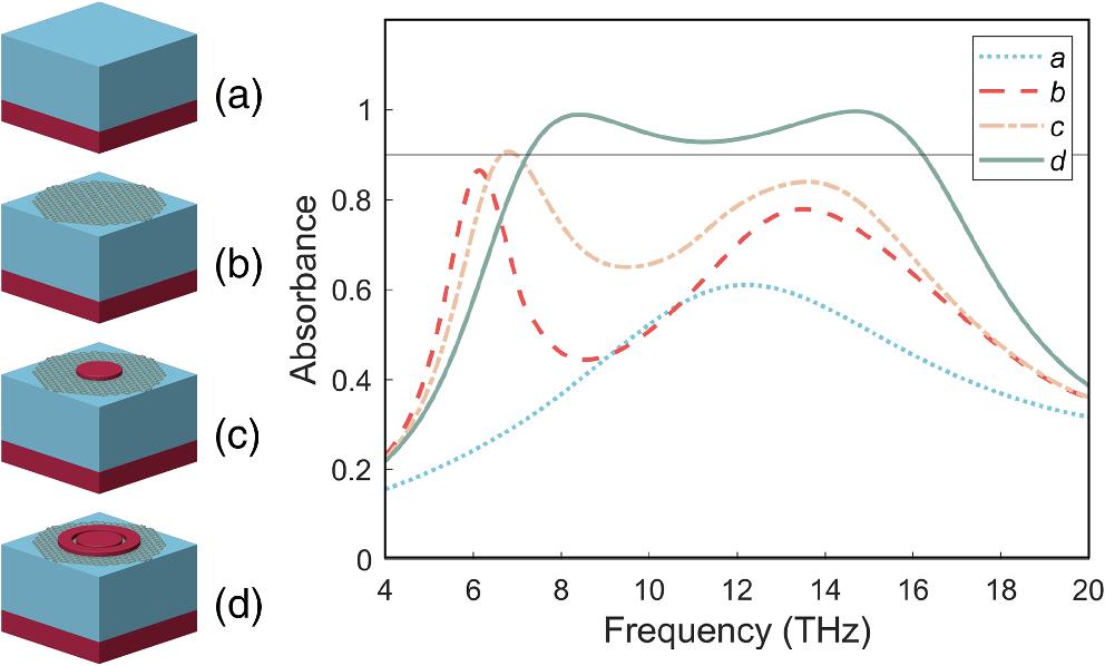
    Fig. 2. (a)–(d) Absorption curves of evolutionary structures (Ef=1  eV).
    (a)–(d) Influence of different structural parameters on the performance of the absorber (Ef=1 eV).
    Fig. 3. (a)–(d) Influence of different structural parameters on the performance of the absorber (Ef=1  eV).
    Absorption curves of the absorber at 0–1 eV graphene Fermi energy levels (the absorption bandwidth at 1 eV is 8.99 THz).
    Fig. 4. Absorption curves of the absorber at 01  eV graphene Fermi energy levels (the absorption bandwidth at 1 eV is 8.99 THz).
    Equivalent parameters (Ef=1 eV): (a) relative impedance, (b) equivalent dielectric constant, and (c) equivalent magnetic permeability.
    Fig. 5. Equivalent parameters (Ef=1  eV): (a) relative impedance, (b) equivalent dielectric constant, and (c) equivalent magnetic permeability.
    (a) split diagram of a unit cell, (b) electrical circuit, and (c) comparison of absorption curves obtained by simulation and ECM (Ef=1 eV).
    Fig. 6. (a) split diagram of a unit cell, (b) electrical circuit, and (c) comparison of absorption curves obtained by simulation and ECM (Ef=1  eV).
    The absolute field distribution and field distribution of vector (Ef=1 eV): (a) E-field (f=8.34 THz), (b) E-field (f=14.66 THz), (c) H-field (f=8.34 THz), and (d) H-field (f=14.66 THz).
    Fig. 7. The absolute field distribution and field distribution of vector (Ef=1  eV): (a) E-field (f=8.34  THz), (b) E-field (f=14.66  THz), (c) H-field (f=8.34  THz), and (d) H-field (f=14.66  THz).
    The power loss (first row) on graphene (left) and graphite (right) and current density (second row) on the top (left) and bottom surfaces (right) in the absorber at frequency (Ef=1 eV): (a) and (c) 8.34 THz; (b) and (d) 14.66 THz.
    Fig. 8. The power loss (first row) on graphene (left) and graphite (right) and current density (second row) on the top (left) and bottom surfaces (right) in the absorber at frequency (Ef=1  eV): (a) and (c) 8.34 THz; (b) and (d) 14.66 THz.
    The absorption spectrum of the absorber (Ef=1 eV): (a) different incident angles of TE mode, (b) different incident angles of TM mode, and (c) different polarization angles.
    Fig. 9. The absorption spectrum of the absorber (Ef=1  eV): (a) different incident angles of TE mode, (b) different incident angles of TM mode, and (c) different polarization angles.
    ParameterValue (μm)
    Unit cell periodicity (P)3
    Width of graphene interconnects (W)0.05
    Radius of graphene structure (R1)1.4
    Outer radius of graphite ring (R2)0.9
    Inner radius of graphite ring (R3)0.6
    Radius of graphite circle (R4)0.5
    Thickness of graphite (T1)0.1
    Thickness of graphene (T2)0.001
    Thickness of dielectric layer (T3)3
    Thickness of substrate (T4)2
    Table 1. Parameters of the designed carbon-based metasurface absorber.
    ReferenceMaterialFrequency range (THz) (A>90%)Bandwidth (THz)Thickness (μm)Insensitive to ΦTunable
    18VO2/metal2.6 to 7.54.976.5YesYes
    21Metal/graphene3.4 to 9.15.79.5YesYes
    47VO2/metal1.85 to 4.32.4512.4YesYes
    36Graphite0.65 to 3.032.3850.2YesNo
    37Graphite6.26 to 13.056.797YesNo
    48Graphene/metal3.69 to 9.776.087.101YesYes
    49Graphene/metal7 to 9.252.255.101YesYes
    This workGraphene/graphite7.24 to 16.238.995.101YesYes
    Table 2. Comparison of performance parameters with those of other absorbers.