• Optics and Precision Engineering
  • Vol. 32, Issue 7, 956 (2024)
Zhaoyu LI, Zihao LIU, Yaoying WANG, Lirong QIU, and Shuai YANG*
Author Affiliations
  • MIIT Key Laboratory of Complex-field Intelligent Exploration, Beijing Institute of Technology, School of Optics and Photonics, Beijing Institute of Technology, Beijing100081, China
  • show less
    DOI: 10.37188/OPE.20243207.0956 Cite this Article
    Zhaoyu LI, Zihao LIU, Yaoying WANG, Lirong QIU, Shuai YANG. High-precision laser confocal measurement of semiconductor wafer thickness[J]. Optics and Precision Engineering, 2024, 32(7): 956 Copy Citation Text show less

    Abstract

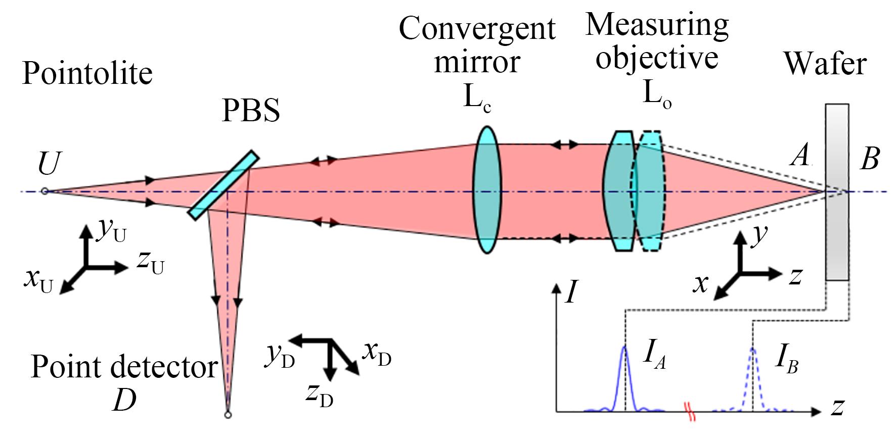
    Addressing the need for precise non-contact measurement of semiconductor wafer thickness, this study introduces a method based on laser confocal technology that ensures remarkable accuracy. It utilizes a voice coil nanodisplacement platform for high-resolution actuation of a laser confocal optical probe, enabling precise axial scanning. This method relies on identifying the peak points on the confocal laser's axial response curve, which are indicative of the objective lens's focal point, to accurately align and position the wafer's upper and lower surfaces. By accurately calculating the physical coordinates of each sampling point on the wafer surface through ray tracing algorithms, this technique achieves high-precision non-contact measurement of wafer thickness. A specialized laser confocal sensor for semiconductor wafer thickness measurement was developed, showcasing an axial resolution of under 5 nm, an axial scanning range of up to 5.7 mm, and repeatability in thickness measurement of under 100 nm across six wafer types. The process takes less than 400 ms for a single wafer. This research successfully applies confocal focusing technology to semiconductor measurement, offering a novel solution for high-precision, non-destructive, online wafer thickness measurement.
    Zhaoyu LI, Zihao LIU, Yaoying WANG, Lirong QIU, Shuai YANG. High-precision laser confocal measurement of semiconductor wafer thickness[J]. Optics and Precision Engineering, 2024, 32(7): 956
    Download Citation