• Acta Optica Sinica
  • Vol. 43, Issue 19, 1928001 (2023)
Xu Nie1, Zujun Wang1,2,*, Baichuan Wang2, Yuanyuan Xue2..., Gang Huang1, Shankun Lai1, Ning Tang1, Maocheng Wang2, Mingtong Zhao2, Fuyu Yang2 and Zhongming Wang2|Show fewer author(s)
Author Affiliations
  • 1School of Materials Science and Engineering, Xiangtan University, Xiangtan 411105, Hunan , China
  • 2State Key Laboratory of Intense Pulsed Irradiation Simulation and Effect, Northwest Institute of Nuclear Technology, Xi'an 710024, Shaanxi , China
  • show less
    DOI: 10.3788/AOS230592 Cite this Article Set citation alerts
    Xu Nie, Zujun Wang, Baichuan Wang, Yuanyuan Xue, Gang Huang, Shankun Lai, Ning Tang, Maocheng Wang, Mingtong Zhao, Fuyu Yang, Zhongming Wang. Experiment and Analysis of Damage of CMOS Image Sensor Induced by Proton Irradiation with Different Bias Conditions[J]. Acta Optica Sinica, 2023, 43(19): 1928001 Copy Citation Text show less
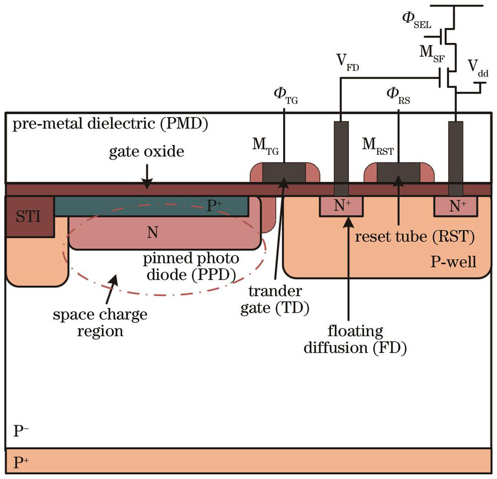
    Section view of pixel unit in 4T PPD type CMOS image sensor[20]
    Fig. 1. Section view of pixel unit in 4T PPD type CMOS image sensor20
    Transient bright spot and lines induced by proton irradiation. (a) Transient bright spot; (b), (c), (d) transient bright lines
    Fig. 2. Transient bright spot and lines induced by proton irradiation. (a) Transient bright spot; (b), (c), (d) transient bright lines
    Particle incident trajectory. (a) Charged particle incident trajectory; (b) proton incident trajectory
    Fig. 3. Particle incident trajectory. (a) Charged particle incident trajectory; (b) proton incident trajectory
    Generation mechanism of CIS dark current
    Fig. 4. Generation mechanism of CIS dark current
    Dark signal output images under different radiation fluences with bias voltage of 5 V. (a) Before irradiation; (b) proton fluence is 1×10¹⁰ p/cm2; (c) proton fluence is 5×10¹⁰ p/cm2; (d) proton fluence is 1×10¹¹ p/cm2
    Fig. 5. Dark signal output images under different radiation fluences with bias voltage of 5 V. (a) Before irradiation; (b) proton fluence is 1×10¹⁰ p/cm2; (c) proton fluence is 5×10¹⁰ p/cm2; (d) proton fluence is 1×10¹¹ p/cm2
    Relationship between dark signal and proton radiation fluence with and without bias voltage
    Fig. 6. Relationship between dark signal and proton radiation fluence with and without bias voltage
    Curve of dark signal varying with proton irradiation fluence
    Fig. 7. Curve of dark signal varying with proton irradiation fluence
    Distribution of pixel counts of dark signal under different proton radiation fluences
    Fig. 8. Distribution of pixel counts of dark signal under different proton radiation fluences
    3D distributions of dark signal spike before and after proton radiation. (a) Before radiation; (b) proton fluence is 1×10¹⁰ p/cm2; (c) proton fluence is 5×10¹⁰ p/cm2; (d) proton fluence is 1×10¹¹ p/cm2
    Fig. 9. 3D distributions of dark signal spike before and after proton radiation. (a) Before radiation; (b) proton fluence is 1×10¹⁰ p/cm2; (c) proton fluence is 5×10¹⁰ p/cm2; (d) proton fluence is 1×10¹¹ p/cm2
    Typical two-level defects in CIS induced by proton radiation
    Fig. 10. Typical two-level defects in CIS induced by proton radiation
    Typical multi-level defects in CIS induced by proton radiation
    Fig. 11. Typical multi-level defects in CIS induced by proton radiation
    Xu Nie, Zujun Wang, Baichuan Wang, Yuanyuan Xue, Gang Huang, Shankun Lai, Ning Tang, Maocheng Wang, Mingtong Zhao, Fuyu Yang, Zhongming Wang. Experiment and Analysis of Damage of CMOS Image Sensor Induced by Proton Irradiation with Different Bias Conditions[J]. Acta Optica Sinica, 2023, 43(19): 1928001
    Download Citation