【AIGC One Sentence Reading】:Metagratings, especially in terahertz domain, offer versatile applications due to their design flexibility and enhanced performances, reviewed with focus on FTTS and sensing.
【AIGC Short Abstract】:Terahertz metagratings, with their simple design and versatile applications, have garnered significant attention. By modifying grating geometry and material characteristics, enhanced device performances are achieved. This article reviews works on antireflection coating, polarization beam splitters, and sensing applications, highlighting FTTS for evanescent wave detection.
Note: This section is automatically generated by AI . The website and platform operators shall not be liable for any commercial or legal consequences arising from your use of AI generated content on this website. Please be aware of this.
Abstract
One dimensional sub-wavelength gratings, also known as metagratings have attracted enormous attention due to the relatively simpler design configurations with versatile application potentials. In recent times, these metagratings have played crucial roles in terahertz frequency domain to realize several fascinating effects. It has been demonstrated that the terahertz characteristics of these metagratings can be modified by carefully designing the grating geometry along with meticulously tuning the material characteristics. Such variations in grating design have led to enhanced device performances. In addition, suitably designed metagratings are capable of exciting strong evanescent orders that can be exploited in ultrasensitive sensing, optical trapping, non-linearity, etc. Based on the tremendous potentials offered by the planar geometry (ease of fabrication) along with diverse utilities, we have reviewed few representative works pertaining to terahertz metagratings in this article. Hence, we have discussed metagratings based antireflection coating and a polarization beam splitter operating in THz region modelled using simplified model method. Further, we have discussed experimental detection of evanescent waves excited in metagratings utilizing Fourier transformed terahertz spectroscopy (FTTS) technique. FTTS is a unique technique because of its ability of simultaneous detection of propagating and non-propagating orders. Next, we have discussed applications of metagratings in sensing trace amount of analytes. Considering the increasing interests in these one-dimensional artificial subwavelength structures, we believe, our article will be useful for the researchers willing to begin work on terahertz subwavelength gratings.
Subwavelength phenomena play critical role in modern day photonics by virtue of their capabilities to transcend the conventional constraints imposed by the wavelength of light. At subwavelength scales where the dimensions of the materials or structures are lesser than the operating wavelength, they exhibit unique optical behaviours that have far-reaching implications in various domains1,2. The scrutiny of subwavelength phenomena within the domain of optics/photonics has created the emergence of artificial materials3−5, most notably exemplified by metamaterials or metasurfaces6−11. Metamaterials are constituted by periodically arranged subwavelength structures/resonators comprising of metal and/or dielectric materials, commonly referred to as meta-atoms12−16. These meta-atoms resonate with the electric, magnetic, or both components of the incident electromagnetic fields17−22. As a result, they demonstrate an effective electric response, characterized by electric permittivity (ε), and/or a magnetic response, represented by magnetic permeability (μ), which does not exhibit naturally. The ability to achieve simultaneously negative electric and magnetic responses and consequently, a negative refractive index23−26 initially sparked intense interest in metamaterials and can be exploited to achieve applications in various areas such as super-resolution27, electromagnetic invisibility28 etc. Likewise, metasurfaces are the two dimensional (2D) analogues of metamaterials where the meta atoms (also called as resonators or antennas) are arranged in 2D periodic array29−39. Metasurfaces offer new degrees of freedom to control the polarization40−43, amplitude44−47, phase46 of the incident radiation in order to achieve wavefront shaping within a distance much lesser than the wavelength. By manipulating the spatially varying optical response upon encountering with light, one can manipulate the wavefront of incident light as desired. The exceptional optical properties and planar nature of metasurfaces have led the development of tunable ultrathin optical devices48−50, exhibiting innovative optical phenomena51−53 or new features that are beyond their conventional equivalents. Apart from manipulating the incident light, metasurfaces have garnered significant interest owing to their utilization in sensing applications54−56, a feat also recently accomplished by topological sensors57,58. However, in such periodic structures at subwavelength scale it is common to see the presence of evanescent fields59,60. Evanescent waves are described as electromagnetic fields with exponentially decaying amplitude where the energy of the evanescent fields remains restricted in the vicinity of the air-grating interface at sub-wavelength scales without the presence of any losses or scattering. Such evanescent waves are widely seen, ranging from optical surface waves such as surface phonon/plasmon polaritons to total internal reflection (TIR) at the interface of two mediums with differing refractive indices61. It has been proposed that evanescent waves can be utilized in many different contexts to take advantage of unique optical phenomena, optical trapping62,63, subwavelength imaging64, fibre optic sensor65,66, biosensing67−69 TIRF (Total Internal Reflection Fluorescent) spectroscopy70, guided optics71, super-resolution microscopy72, cooling73, and so on. One of the relatively simpler devices that predominantly excites and allows one to harness the energy of evanescent fields is metagrating. As demonstrated earlier74 metagratings can sustain stronger resonant evanescent orders. In case of metagratings, all the higher order propagating modes are absent while only the zeroth order mode propagates energy into far-field, discussed in details in Section Physics of metagratings.
On the other hand, in recent decades, there has been a growing focus on the terahertz (THz) waves, which represents a novel opportunity for interactions between light and matter at relatively low photon energy. This is attributed to its unique position within the electromagnetic spectrum75,76. THz radiations (typically 0.1 THz to 10 THz) occupies a position within the electromagnetic spectrum that lies between infrared and microwave radiations, and exhibits certain characteristics that are common to both the infrared and microwave radiations. Similar to infrared and microwave radiations, THz radiation propagates in a line of sight and is non-ionizing. Much like microwave radiation, THz radiation has the capability to penetrate through a diverse range of non-conductive materials. Moreover, THz radiations possess exceptional characteristics such as wide bandwidth77, non-invasive78−80, higher resolution81, etc. Nonetheless, the THz technology still lacks due to the unavailability of suitable devices and there is significant amount of ongoing efforts to realize THz compatible devices82,83. However, this limitation hinders the effective utilization of THz frequencies in several fields. Therefore, metagratings (subwavelength gratings) functioning within the THz regime hold significant potential for advancing the field of THz, offering numerous avenues for development. In addition to enriching the domain of THz sciences, this will aid in the development of innovative devices for the THz region, which have applications in a number of domains, including imaging84,85, beam steering86,87, detection88,89 and communications90−93. Considering the current surge in metagrating studies, here, we provide a perspective on the physics and applications of metagratings primarily focussed on THz frequency domain. The review is broadly organised as described below, Section Physics of metagratings describes the physics of metagratings and current utilities of the metagrating, Section Applications discusses several signature applications of dielectric metagrating operating in THz domain and Section Summary and outlook summarizes the review briefly with future scopes.
Physics of metagratings
The diffraction gratings play a crucial role in optical systems due to their exceptional characteristics such as dispersion of incident light into a spectrum of associated wavelengths or steering of incident light into desirable direction by utilizing a periodic structure (Fig. 1). It is an assortment of transmitting or reflecting elements separated by a distance corresponding to the wavelength of the incident light under investigation. In diffraction gratings, the modulation of amplitude and phase of the incident light is achieved by spatial variation of refractive index. Because of the ability of gratings to distribute energy in different diffraction orders, they have been applied in the development of versatile spectroscopic tools and other relevant areas extensively94−96. Over the years, gratings have been categorized into different types, such as transmission, sinusoidal, holographic, blazed, triangular, concave, and various others according to their geometry, efficiency behaviour, materials and applications97. The simplest form of a grating structure consists of periodic arrangement of rectangular bars of finite thickness with two different refractive indices in one dimension98. Commonly, there are four different refractive indices involved in a simple grating, low refractive index bar (groove), high refractive index bar (ridge), the area below the grating and area above the grating surface. When light is incident on the grating, it is diffracted in several orders of both reflected and transmitted waves. The classical phenomenon of diffraction by a simple grating can be visualized in Fig. 1(a). In effect, each groove becomes a tiny source of transmitted or reflected waves. The diffracted orders are exhibited at deviating angle to the grating surface (Fig. 1). The wavelength of the incoming wave, the periodicity of grating, and the angle of incidence are the usual factors that determine the number of diffracted orders, this can be explained by the grating Eq. (1), also known as Fraunhofer equation99,
Figure 1.(a) The phenomenon of diffraction through conventional diffraction grating, where higher diffraction orders are present. (b) The diffraction phenomenon from metagrating where higher orders become evanescent in nature and only the zeroth order mode propagates light in the far-field.
where d is the periodicity of grating, θm and θi are angle of diffraction and angle of incidence respectively, λ is the wavelength of the incident wave, and m is an integer which specifies the number of diffracted orders. For a given set of grating period, incidence wavelength and incident angle, the grating equation can only be solved for a wide range of values of m when |sinθm|<1. Such diffraction modes are called propagating modes. On the contrary, if the periodicity of the grating becomes smaller than the wavelength of the incident wave (d < λ), it results in an absence of a genuine solution for θm. Consequently, only the zeroth-order mode (propagating mode) manifests in the far field, eliminating diffraction effects while, the higher-order modes give rise to a non-propagating electromagnetic field in close proximity to the grating surface, called as evanescent waves. This class of grating is termed as subwavelength grating or meta-grating (Fig. 1(b)). As light travels through the metagrating, it undergoes a behaviour closely resembling that of traversing a uniform medium and their response can be modelled using effective medium theory100−102. These metagratings can be fabricated by various processes amongst them a most commonly used method is photolithography. In photolithography, the photoresist is spin coated onto the silicon wafer on which the device design has to be patterned. Subsequently, the design of the device is imported from a photomask. Afterwards, the resist coated silicon wafer is exposed to ultra-violet light by employing the photomask and developed, to imprint the pattern. For dielectric metagratings, followed by resist patterning, deep reactive ion etching is utilized to etch out the grooves. While for metal gratings, metal is deposited followed by lift off. In recent years, metagratings have been studied extensively and the evanescent wave excited through these subwavelength gratings are utilized in many different applications to take advantage of cutting-edge optical effects103. Some of the applications include transmission colour filters104, biosensing105−108, optic fibre couplers109, resonant transmission of infra-red110, apertureless microscopy111,112, and high efficiency light emitting diodes113, nanoelectromechanical devices114, etc.
Considering the simplicity in metagrating’s geometry and rich physics involved, these photonic structures have undergone both theoretical and experimental examinations, finding applications in deflectors, holograms, sensing, and various other domains. Although metagratings are generally well exploited in optical and infrared domains but studies in THz is limited so far. However, in recent times, THz metagratings are being explored by few groups around the globe. Therefore, we discuss few applications of THz metagratings below.
Applications
Antireflection coating
In THz experimental set ups, numerous components rely on high refractive index substances such as silicon, leading to significant reflection losses occurring at the interface. This creates the demand for antireflection coatings in THz domain. Typically, in visible region, antireflection coatings are made up of quarter wave dielectric coatings with the condition that its refractive index must correspond to the square root of the multiplication of the refractive indices of both the surrounding medium and substrate material116. However, it is difficult to find the suitable dielectric materials as quarter wave coatings in THz domain and the long wavelength of the THz waves results in the need for thicker coatings. In this regards, various functional devices such as two dimensional (2D) antireflection metamaterials117 and metagratings are developed to manipulate the THz waves in order to attain the antireflection coating118,119. The 2D pyramidal gratings provide antireflection properties with wide bandwidth and high efficiency by forming a monotonous index transition from air to material, basically controlling the Fresnel coefficients. However, the fabrication of such 2D gratings is cumbersome considering the complex non-smooth profile. Therefore, in view of the need for simpler antireflection coatings. Ma et al. have designed and fabricated dielectric based polarization insensitive antireflection structure in THz domain115. Here, the antireflection structure is attained by configuring the grating parameters in a way that creates an effective Fabry-Perot resonator, resulting in simultaneous minimization of transmittances for both the TE and TM waves. The metagrating can be modelled as a homogeneous layer of dielectric slab with effective refractive index and the diagrammatic representation of the modelling is shown in Fig. 2(a). It can be seen that when the metagrating is considered as a slab of dielectric, it acts as Fabry-Perot resonator which can be modelled by utilizing simplified modelled method (SMM). When the grating period is significantly lower as compared to the wavelength of the incident light, typically only a single propagating mode persists within the grating regime while higher-order modes become evanescent and are thus typically disregarded. By employing the effective medium theory, the subwavelength grating can be considered as a slab of homogeneous medium. Consequently, one can derive the transmission and reflection characteristics of the grating by employing Fresnel's equations (which is typically called as SMM)120−122.
Figure 2.(a) The schematic illustration of grating and the equivalent effective medium structure. When the grating is considered as homogeneous slab having effective refractive index, the grating region acts as a Fabry-Perot resonant cavity exhibiting multiple total internal reflections. The obtained transmittance characteristics of the proposed grating design for (b) TE and (c) TM polarization as a function of frequency. Here, the black solid line represents the transmittance acquired through numerical simulations while the red dotted line represents the transmittance obtained from experiment. The slight variation in the transmittance for both the polarizations (TE and TM) can be attributed to the different effective refractive indices for both the configurations. Figures reproduced from: ref.115, Elsevier B.V.
In case of reverse engineering, the use of SMM can significantly boost the design process. The SMM simplifies the process of determining optimal groove depths for maximum transmittance across grating with varying fill factors and polarizations. In order to avoid the higher order diffraction modes, it is necessary to select a set of groove depths and fill factors that work effectively for both TM and TE polarizations. Subsequently, COMSOL is employed to optimise the parameters for precision. The metagrating design with optimized parameters is fabricated using lithography followed by deep reactive ion etching. Initially, the predetermined design pattern underwent importation into a laser writer for the creation of the mask. The subsequent stage involved the pre-processing of the silicon wafer through a combination of heating and washing procedures. Following this, a 10 μm thick positive photoresist film was applied to the wafer using spin-coating techniques. Following the lithography process, the wafer underwent development in developer followed by thorough rinsing with deionized water. Further, a deep reactive ion etching process facilitated the etching of the wafer, resulting in the formation of the desired grating. Lastly, any residual photoresist is removed using acetone. THz time domain spectroscopy is employed to study the far-field transmittance. The experimental and simulation transmission are contrasted in Fig. 2(b) and 2(c) for TE and TM incidences respectively. It can be seen that the transmittance characteristics are dominated by Fabry-Perot oscillations. At around 0.87 THz, the transmittance for both TE and TM case is observed to be 84% and 94% respectively. The difference between the experimental and the simulation results is a consequence of fabrication error in the grating parameters. The outcomes demonstrate that the metagrating effectively reduces the reflectance at a single silicon-air interface, decreasing it from 30% to 5% for the TM wave and 15% for the TE wave and. Hence, it demonstrated significant reduction in THz reflections for both the polarizations.
Another example, where Ding et al. experimentally demonstrated an antireflection coating for THz radiation by employing a thin metallic grating with deep subwavelength periodicity123, where it has been shown that the chromium (Cr) lamellar grating effectively eliminates the internal reflection of a broadband THz pulse, occurring at a Si/air interface. The lamellar gratings proposed in this work are designed to have a periodicity of 10 μm and variable thickness between 10 nm to 60 nm. THz-TDS in transmission configuration is used to characterise the samples and Fig. 3(a) depicts the acquired transmitted signals through Cr metagrating and silicon substrate (reference). Here, P1 represents the primary pulse that has travelled through the sample (main pulse), while P2, exhibiting a delay of around 7.5 picoseconds, signifies the THz pulse transmitted subsequent to completing a single internal reflection cycle within the silicon substrate (etalon pulse). The reflection coefficient pertaining to the silicon surface can be expressed as. With the grating parameters as thickness (d)=25 nm and fill factor (u)=0.35, it is observed that in case of TE polarization, the P2 pulse almost disappears, representing low reflection at the Si/grating/air interface. Conversely, P2 maintains its amplitude unchanged under TM polarization when contrasted with the scenario of bare silicon, suggesting the presence of a reflection coefficient depending on polarization. The decrease in P1 transmission in TE polarization is due to a 67% absorption in the antireflection layer whereas, the transmission remains unaffected at 100% in TM polarization, with absorption being negligible. The underlying physics revolves around the distinct effective complex refractive index observed for TE and TM polarizations within metallic gratings.
Figure 3.(a) The THz-TDS transmission signals have been observed under normal incidence. The solid curve represents bare Si, while the dashed and dotted curves depict Si coated with antireflection grating in TE and TM polarizations, respectively. (b) The amplitude and (c) phase shift of the complex reflective coefficient are measured at the Si/grating/air interface at 0.75 THz, with incidence being normal from the Si side. The noise level of the THz-TDS system is currently overlaid. Analytically calculated results for TE and TM waves at Cr thickness d = 30 nm are depicted as solid and dashed curves, respectively. Error bars are utilized to denote the geometric uncertainty arising from grating fabrication. Figures reproduced from: ref.123, Wiley-VCH GmbH.
Further, to examine how the reflection coefficient at the Si/grating/air interface varies based on grating parameters (d, u), a series of gratings with the thickness of 25 nm and varying fill factor between 0.3 to 0.6 are measured. The amplitude |rc| and phase shift φc of complex reflection coefficients for TE and TM polarization measured at 0.75 THz are shown in Fig. 3(b) and 3(c) respectively. For the TE polarization, |rc| reaches its lowest value of 0.042 at the point of reflection minimum, where u = 0.35, representing a significant reduction in reflectance, approximately 99% lower compared to the reflection from a bare Si surface. As the value of u increases above u = 0.35, the |rc| steadily increases, reaching 0.55 for an uncoated Si surface (u = 0), and 0.41 for a surface coated with a Cr-film (u = 1). Regarding φc, there is a swift transition from 0 to π as u crosses u = 0.35. φc = π for TE (φc = 0 for TM) signifies the trait of reflecting back to an optically denser medium. In this scenario, the impedance of air has been excessively compensated by the Cr film or grating, resulting in the incident field from the Si side encountering a medium with a reduced effective impedance. At φc = π/2, the impedances of silicon and air align with the respective chromium grating coatings, achieving the ideal antireflective state. Moreover, for TM polarization, |rc| is approximately 0.45 for u ranging from 0.3 to 0.6, and φc is nearly π. Therefore, the reflective properties of the Cr grating-exhibit a decrease of over 99% when compared to the bare Si sample across the entire bandwidth range of 0.06–3 THz utilized by the THz TDS system.
Beam splitter and retroreflector
One of the fascinating fact about grating is that it has the capability to redirect incident light/EM wave into various diffraction orders99. This feature opens up potential applications in Polarizing Beam Splitters (PBS) designs. Taking into account this feature of grating, Ma et al. has proposed a metagrating design of THz PBS that relies on SMM124 and experimentally investigated its efficiency by utilizing THz time-domain spectroscopy. The SMM contributes valuable physical insights and theoretical overview for the design of grating. As discussed in the introduction, typically metagrating can be operated in zeroth order propagating modes while higher order modes can be made evanescent in nature. However, there can be more than one propagating diffraction order depending on the design of the device, for instance by manipulating periodicity or refractive indices. Therefore, the SMM has been utilized to model the diffraction phenomenon by considering it as the interference resulting from the two modes of propagation, in a manner similar to that utilized in a Mach-Zehnder interferometer. The diffraction phenomenon and the equivalent interference process is depicted in Fig. 4(a). In a Mach-Zehnder interferometer, an incoming wave undergoes a bifurcation into two identical waves, subsequently traversing distinct paths or materials and the resultant wave leaves the interferometer through either port 1, port 2, or both. The emitted wave intensity is dependent on the optical path differences between the two divergent waves. Notably, interference occurring within the grating closely resembles as found in the Mach-Zehnder interferometer, assuming no reflection at the grating input. Although the two propagation grating modes posses different effective refractive indices, they share the same propagation length. Consequently, these modes develop a phase difference akin to the two split beams in the Mach-Zehnder interferometer. Moreover, the optical path difference also governs the efficiency of the diffraction orders, the condition for the diffraction mode to leave the grating from 0th order, the phase difference is supposed to be zero (starting from the substrate).
Figure 4.(a) Schematic representation of a two-mode SMM used to depict the metagrating as a Mach-Zehnder interferometer without taking reflection of grating into account. Two-dimensional maps of the experimentally measured efficiencies of the grating device with frequency and angle for (b) TE and (c) TM configuration. In both the cases the metagrating is illuminated at Littrow angle of 46°. Figures reproduced with permission from: ref.124, under the terms of the Creative Commons Attribution License (CC BY).
To validate the proposed design authors have experimentally measured the diffraction efficiencies of the proposed metagrating design by employing fibre laser based THz time domain spectroscopy. The obtained temporal signal measurement is subsequently converted into the frequency domain using a fast Fourier transform for analytical purposes. Figure 4(b) and 4(c) show the two-dimensional plot of angle resolved diffraction efficiencies for TE and TM waves respectively. While the intention of the design is focused on a singular frequency, the metagrating manifests its diffractive characteristics when subjected to broad-spectrum THz wave illumination. As can be seen in Fig. 4(c) the TM wave experiences first-order diffraction within a frequency range centred around 0.9 THz and the diffraction angle increases with longer wavelengths. In relation to the transmittances of a silicon plate at an incidence angle of 46°, the diffraction efficiency for TE and TM waves are 69% and 63%, respectively. This outcome emphasizes that suitable and innovative metagrating designs can probably out perform a silicon-based PBS.
For retroreflection, Cheng et al. proposed a novel design of metagratings with an accordion-like structure, tailored for retroreflection in the THz domain87. Retroreflection represents a unique form of beam manipulation wherein the reflected beam is redirected back towards the incident direction across a specific range of incident angles. This process holds significant importance in augmenting backscattering effects and aiding in signal tracking improvement. In order to facilitate retroreflection, it is imperative to continuously tune both the direction and momentum of the incident wave. The majority of reported metasurfaces exclusively offer retroreflection at one specific incident angle owing to the consistent momentum125,126. Whereas the proposed metagrating accordingly designed in a way to provide retroreflection across a broad spectrum of incident angles by tuning inter-element distances via mechanical compression and stretching of the metagratings. The cross-sectional view of the proposed metagrating design is depicted in Fig. 5(a). The ridges are connected at both extremities in a zigzag pattern to facilitate compression. At a particular incident angle, the metagrating undergoes compression to the degree that the momentum it imparts equals twice the incident momentum but in the opposite direction (p = −2pi). Consequently, the reflected beam acquires the momentum equivalent to −pi, returning towards its original incident trajectory. The periodicity of metagrating is connected to the retroreflection angle (θr) as Λ = λ/2sinθr, where Λ is periodicity of the grating and λ is the wavelength of the incident wave. Hence, the −1st diffractive pathway is associated with retroreflection, while the 0th order pertains to specular reflection. For a chosen set of width and thickness parameters as 0.85 and 3 mm, respectively, the simulated retroreflection efficiencies exceed 60% for angles between 40° and 89°, while nearing 100% for angles ranging from 55° to 84° as shown in Fig. 5(b). This highlights the exceptional characteristics of high efficiency and a broad angular range. For experimentation, the dielectric metagrating is fabricated via 3D printing and is affixed onto an aluminium plate with a thickness of 0.5 mm. Subsequently, compression is applied to the dielectric metagrating while keeping the aluminium plate stationary throughout the measurement process. The retroreflected light is detected by a beam splitter, which comprises a high-resistance silicon wafer, using a Schottky diode detector positioned on a 3D translation platform. Initially, the incident light is directed towards the aluminium plate, with the reflected light serving as the reference for achieving ideal retroreflection. Subsequently, the 3D-printed metagrating is affixed to the plate and adjusted to various incident angles. For each angle of incidence θi, the metagrating undergoes compression to such a degree that the resulting beam spot appears at its maximum brightness when measured. The retroreflected beam spots are measured when θi is from 45° to 65° with 5° steps and is shown in Fig. 5(c). The metagrating dimension extends to 80λ in its relaxed state, thereby ensuring the absence of beam leakage, even when subjected to an incident angle as steep as 65°. To summarise, an innovative angle-responsive retroreflector is showcased, exhibiting effectiveness across incident angles ranging from 45° to 65°, achieving a recorded peak efficiency of 77%.
Figure 5.(a) Cross-sectional view of the proposed metagrating design and illustration of dynamic angle adaptive retroreflection. Modifying the period of the metagrating facilitates the provision of the desired momentum for various retroreflection angles. (b) The retroreflection efficiency obtained via simulated and experiment over a wide range of incident angles. (c) The reflective intensity distributions are assessed by measuring them from both an aluminium plate (used as a reference) and a retroreflector, considering various incident angles and periods respectively. Figures reproduced from: ref. 87, Wiley-VCH GmbH.
When dealing with the detection of trace amount of analyte, traditional THz sensing encounters challenges due to the large parity between the wavelength and the dimensions of the sample. Therefore, the use of THz metastructures in sensing or detection helps to overcome this problem by providing enhanced light matter interactions127,128. The THz sensing is complex as the THz metastructure has much larger surface undulation and demands interface engineering to achieve the conformal coating of ultra-thin trace-amount analytes onto the metastructure. In addition, even with a perfect conformal sample coating, variations in the strength of the electric field may result in nonuniform fingerprint absorption throughout the sample surface. The efficiency of the interaction between light and matter in sensing applications may be reduced by this non-uniformity. Therefore, it is imperative to develop a sensor that has a higher sensing efficiency in order to improve the THz range broad-spectrum molecular fingerprint detection for trace analytes. Thus, Liu et al. has recently proposed a metasensor129 that achieves high performance through the generation and utilization of evanescent waves by employing a simple dielectric metagrating design. As discussed in section Physics of metagratings, metagratings allow energy propagation exclusively in the zeroth diffraction order while the higher orders can support only the evanescent orders. Although these evanescent orders do not participate in transmission of energy but can act as reservoir of huge energy trapped near the grating interface. Hence, any little perturbation on evanescent fields leads to a significant alteration in the field strength. Therefore, the proposed metasensor enables the detection of molecular fingerprints in the THz (THz) range for a wide range of trace-amount analytes deposited on a flat sensing surface.
Therefore, a homogenous SiO2 dielectric metagrating in reflection mode is utilized as metasensor to detect several analytes such as histidine, α-lactose, MXene, etc. Figure 6 shows the detection of the α-lactose where Fig. 6(a) represents the complex refractive index of the α-lactose. To unveil the capabilities of the proposed metasensing technology, the impact of three different sample coating scenarios on the performance of fingerprint detections are studied numerically by utilizing rigorous coupled wave analysis (RCWA) and finite element method based COMSOL Multiphysics. The schematic illustration of the three cases of coatings is illustrated in Fig. 6(a). The peak envelopes and reflectance spectra for the three coating scenarios are depicted in Fig. 6(b), and 6(c), correspondingly. The peak envelopes generated by the samples in all three scenarios exhibit a dip at approximately 0.53 THz which attributes to the frequency at which the extinction coefficient for α-lactose reaches its maximum. The electric field distributions for each case are shown in the insets of Fig. 6(b) and 6(c). The presence of the analyte results in the absorption of THz waves, diminishing the electric field intensity in the surrounding area at the resonance frequency. This study claimed a 303 times improvement in fingerprint detection performance when compared to previously reported methods for trace amount of analyte130,131. The improvement in sensing can be accredited to the utilization of evanescent waves at the interface between the air and the metagrating.
Figure 6.(a) The top left figure denotes the complex refractive index of α-lactose sample, where the red and blue line represents real and imaginary part of the refractive index. The rest three figures denote the three surface coating instances for trace sample of equal volume. (b) The envelope corresponding to the angle-multiplexed reflectance spectra for conformal analyte coating and (c) The envelope associated with the angle-dependent reflectance spectra for evenly coated surface. The insets of the figure represents the normalized electric field distribution. Figures reproduced with permission from: ref. 129, under a Creative Commons Attribution 4.0 International License.
For another verification of trace amount of analyte sensing by utilizing THz metagrating, Xie et al.132 proposed an angle-multiplexed fingerprint sensing based on a series of guided mode resonances. Metagratings employing parameter-based multiplexing possess an ability to leverage various resonance peaks produced by diverse angles of incident waves to enhance the interaction between the wave and the material, particularly as the peak values of these resonances alter with the absorption spectrum of the analytes. In this work, a silicon metagrating (periodicity =15 μm) with a gold mirror coating at the back (see Fig. 7(a)) is utilized to sense a trace amount of Ta2O3. The incorporation of a gold mirror within the lossy silicon metagrating plays a pivotal in enhancing the detection of broadband THz fingerprints. Typically, in metagratings the angle-multiplexed zeroth mode of +1 order guided mode resonance is employed to extract the molecular fingerprint131. Here, the metagrating is fabricated via photolithography followed by inductively coupled plasma etching, while gold and Ta2O3 is deposited by using magnetron sputtering. Further, a THz-TDS system has been employed in reflection mode for measuring the angle-multiplexed spectra of the samples and the obtained absorbance envelop is shown in Fig. 7(b). Due to the fact that the refractive index of Ta2O3 is higher than that of air, there is a noticeable shift in the series of GMR absorbance peaks towards lower frequencies. Additionally, the frequency corresponding to the highest absorbance peak also shifts towards the characteristic fingerprint point of Ta2O3. The resulted fingerprint signal is depicted in Fig. 7(c) and has a peak frequency at around 0.51 THz indicating the spectral absorption feature of Ta2O3. The intensity of the fingerprint signal acquired from an unpatterned silicon substrate is notably weak (the blue dashed line in Fig. 7(c)), rendering it difficult to distinctly distinguish against the prominent fingerprint peak. The absorbance at the fingerprint frequency of 0.51 THz has experienced a remarkable increase up to 98 times. The aforementioned findings illustrate that this approach has proven effective in facilitating the THz fingerprint detection of trace thin film samples.
Figure 7.(a) Proposed metagrating design with a gold mirror at the back. The schematic denotes various parameters: θ signifies the incident angle, n denotes the number of angles, w represents the unit cell period, p indicates the grating layer width, h1 pertains to the height of the grating layer width, and h2 denotes the height of the waveguide layer. (b) Absorbance envelop of Ta2O5 thin film (1-µm thickness). (c) The fingerprint signal of the Ta2O5 film. Figures reproduced from: ref.132, IEEE.
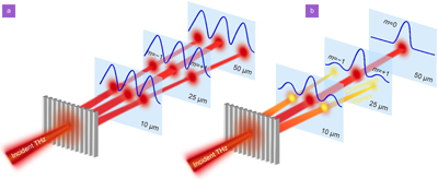
As previously discussed, evanescent waves can be advantageous in sensing and numerous other applications. However, the excitation of the strong resonant evanescent orders and their experimental detection is cumbersome task due to the small scale and non-propagating nature of the evanescent waves. Thus in this regards, in another work, a dielectric metagrating design is pursued and explored in one dimension to leverage the evanescent orders for orthogonal polarizations (TE & TM both) of incoming THz radiations, examining the impact of grating height (while maintaining a constant fill factor) on the generated evanescent orders133. In order to achieve this, near-field THz spectroscopy in employed in conjugation with extra ordinary utility offered by Fast Fourier transformations. This unique combination is termed as Fourier Transformed Terahertz Spectroscopy (FTTS). This special combination facilitates insights into the exploration of resonant evanescent orders within the THz domain, manifesting at length scales significantly smaller than the operational wavelength (~ λ/20).
In this investigation, a one-dimensional silicon grating with 100 μm periodicity is used to excite and exploit the evanescent orders. In order to experimentally capture the evanescent orders, it is necessary to obtain a picture of the diffraction profile of the designed grating. Therefore, with the aim of comprehending the diffraction profiles of the designed metagratings, electric field intensities are measured at several distances away from the grating interface using Near-field Scanning Terahertz Microscopy (NSTM) across the frequency range spanning from 0.2 THz to 0.9 THz. The NSTM records electric field variations as a function of time at distances along the grating vector. Further, this data is transformed into frequency domain response through the application of FFT. Applying Fourier transformation on the recorded electric fields offers a perspective on both the non-propagating and propagating diffraction modes across a wide frequency spectrum, revealing the diffraction profile of the grating in momentum space (k-space). In this context, the diffracted orders may manifest as either negative or positive integer values (m = ±1, ±2, ±3, ...), where m being 0 represents the zeroth order, corresponding to the propagating mode. The diffraction profile derived from experimental observations of the grating, operating within the 0.2 THz to 0.9 THz frequency range in both TE and TM configurations, are illustrated in Fig. 8. Here, the blue dotted line represents the boundary for the subwavelength domain in momentum space (k-space), this can be calculated by using grating equation (see, Eq. (1)). The diffraction modes within the blue lines represent propagating modes with moduli of 2π/λ, while the higher-order modes outside the subwavelength regime exhibit evanescent characteristics. As evident from Fig. 8, the central bright peak (m=0) transmits energy into the far-field region, while diffraction modes beyond the subwavelength range (m=−1, m=1) neither transmit energy into the far-field nor exhibit a sustained presence away from the interface, demonstrating their evanescent nature. Moreover, to confirm the evanescent characteristics of the higher diffraction orders, the peak electric field values for these orders at varying distances from the grating interface have been plotted. This was done for both the incident polarizations, and the results are illustrated in Fig. 8(g) and 8(h). Exponential decay fitting is employed to model the decay characteristic of higher orders based on the observed data. The experimentally measured decay lengths of the evanescent orders in the TE and TM configurations are observed to be 18.21 µm and 12.61 µm, respectively. The findings from both experimental measurements validates the exponential decay nature exhibited by higher-order modes within spatial dimensions significantly smaller than the wavelength (< λ/20). Further the design of the metagrating is optimized with the help of numerical simulations to excite prominent evanescent orders. Hence, the current study can be promising in characterizing the evanescent orders by employing simpler grating design which can be utilized in various fields such as sensing of ultra-small particles and biomolecules (DNA, protein, etc.), super-resolution72, non-linearity etc.
Figure 8.The diffraction patterns of the experimentally acquired findings across the frequency spectrum from 0.2 THz to 0.9 THz after utilizing Fast Fourier Transform (FFT). The diffraction profile for TE incidence is shown by (a–c) for difference distances (10 μm, 20 μm, and 50 μm) away from the grating surface (along Z), whereas the diffraction profile for TM incidence is represented by (d–f). (g) and (h) illustrate the exponential decay characteristics of the +1 evanescent order, derived from experimental measurements for TE and TM cases, respectively. Here, the error bars signify variations in the experimental data, potentially arising from deformities during fabrication processes. Figures reproduced with permission from: ref.133, under the terms of the Optica Open Access Publishing Agreement.
As discussed in section Physics of metagratings, metagratings are capable of manipulating the light, where the incident power can be rerouted towards the single desired diffraction order with optimal efficiency (unitary efficiency) while suppressing the undesired diffraction orders. In this regard, Younes Ra’di et al. has proposed a metagrating design134 providing a reconfigurable platform tuned by the electrostatic biasing of graphene sheets with much lesser fabrication complexity. In case of typical graded metasurface, the direction of the incident wave is changed by employing gradient of surface impedance to locally change the (reflection) phase whereas metagrating adopt a distinct strategy that possess the ability to redirect incoming waves with optimal efficiency. A carefully designed metagrating orientates the direction of one of the propagating higher-order floquet modes in line with the desired reflection direction, transferring transverse momentum to the surface instead of through a gradient in the local reflection coefficient. Recently, the approach involving metagratings has demonstrated the capability to achieve highly efficient manipulation of waves with unitary efficiency. In this work, Younes Ra’di et al. extended the previously introduced approaches135, where the required channels in reflection may be selected using a conventional diffraction grating method, and the electromagnetic response of each individual complex inclusion inside each unit cell can be tuned to ensure unitary efficiency for any wavefront manipulation. Based on this approach authors have put forward a configuration capable of inducing comparable asymmetric scattering in a more straightforward manner Moreover, this streamlined configuration is utilized to achieve the implementation of reconfigurable metagratings, leveraging the properties of graphene. For the reconfigurable platform, the proposed structure uses a unit cell design that consists of two graphene sheets controlled by separate bias voltages and four metallic strips. The schematic view of the proposed device design is shown in Fig. 9(a). In case of static configuration (without graphene sheet), null (zero) radiation in desired direction is achieved by breaking radiation symmetry of the structure. For the purpose of disrupting symmetry, the metal strips with different design parameters are employed, these strips resonate at frequencies that exhibit slight variations. Whereas in case of reconfigurable design (with graphene sheets), one can tune the effective conductivity of the graphene strips by altering the chemical potential of these strips, leading to the eventual modulation of two resonance frequencies of the unit cell.
Figure 9.(a) Illustrative depiction of graphene based reconfigurable metagrating. Results for two different cases where (b) and , (c) with design parameters p = 60.926 µm, w = 19.4 µm, s = 5 µm, g = 2.9 µm, h = 8.5 µm, q = 0.05 µm. Here the blue, green and red lines represents the transmittance for 00, 0(–1) or 01 diffraction modes respectively. Figures reproduced from: ref.134, American Chemical Society.
The response of the metagrating comprising the graphene sheet is studied numerically by utilizing the CST Microwave Studio and the designated frequency for all instances is 5 THz. The studies are carried out for two different cases, for the case I, the chemical potentials for sheet a and sheet b are 1.3 eV and 0.63 eV, respectively, and 0 eV in case II. The results obtained for case I are depicted in Fig. 9, illustrating outcomes acquired for three different incidences. In Fig. 9(b), the left panel illustrates the redirection of the incident wave towards the intended direction, achieving an efficiency of over 80%. In the middle panel, it is evident that, owing to reciprocity, the identical configuration reflects the incident wave originating from θinc = 80° back towards a direction perpendicular to the metagrating at θref = 0°. If the excitation is from the angle 0(−1) with an incident angle θ = –80°, the layer will function as a retroreflector. This results in the reflection of the entire incident wave, with the exception of the dissipated power, directed back toward the source at θ = –80°. In case II, the voltage of graphene layers is set to be zero and the results are depicted in Fig. 9(c). The left panel of Fig. 9(c) demonstrates that the metagrating functions as a traditional reflector when stimulated by a normally incident plane wave. Whereas if the metagrating is excited from other two directions (0(1) or 0(–1) modes), part of the power is reflected back to the source, while the remainder is transferred into the 0(–1) and 0(1) channels. Therefore, it is evident that with relatively simpler geometry of metagrating one can achieve highly effective redirection of incident light to extreme angles while operating in the reflection mode.
Metagratings in other frequency domains
While we have focused this review extensively on metagratings operating in THz domain, we have as also shed a light on their utilization across the other domains of the electromagnetic spectrum.
i) Beam splitter
A multifunctional phase gradient metasurface (PGM) based light beam splitter in the optical regime is designed and investigated by Xie et al. by manipulating the diffraction properties of the metagrating136. As recognized, PGMs represent periodic gratings characterized by a supercell consisting of unit cells exhibiting distinct optical behaviours, discretely inducing a abrupt phase shift covering a full 2π. The introduction of the abrupt phase shift leads to the emergence of a phase gradient, thereby introducing an extra wave vector in fundamental principles governing the reflection and refraction of light at the interface46. The phenomenon of diffraction is widespread in PGMs, as evidenced by numerous studies28−30, wherein higher-order diffraction is elucidated by a diffraction law dependent on parity31. Hence, achieving unrestricted control of diffraction phenomena within PGMs, along with enhancing their efficacy. In this regard, a gradient metallic grating having a phase gradient at the transmitted interface is designed and the schematic is illustrated in Fig. 10. To demonstrate the polarization splitting properties of the devised metagrating, the electromagnetic field distributions at the incident angles θi = ±30° are presented through COMSOL Multiphysics simulations. Figure 10(b) and 10(c) display the total magnetic and electric field patterns calculated numerically for an incident angle of θi = −30°, corresponding to TM and TE polarized light, respectively. The directional orientation of the incidence and specular reflection of the n=0 order is denoted by the black arrows in the figures. The blue arrows delineate the orientations of the anomalous transmission with an index of n=−1. It is evident that TM polarized light exhibits highly efficient negative refraction, while TE polarized light demonstrates perfect specular reflection. Currently, the polarized light separated into TM and TE components is positioned on both facets (namely, the areas of reflection and transmission) of the metagrating. Therefore, through the examination of the diffractive properties of various orders and the parity of the metagrating, the devised metagrating demonstrates the capability to accomplish efficient polarization-based light beam splitting.
Figure 10.(a) Illustration of the polarization beam splitter constructed using a metallic metagrating. (b) Magnetic field configuration observed at an incident angle of θi = −30° for light polarized in the TM configuration. (c) The electric field configuration at an incident angle of θi = −30° for TE-polarized light. Figures reproduced with permission from: ref.136, under the terms of the Optica Open Access Publishing Agreement.
In the majority of sensing applications that rely on resonance shifts, sensitivity and resolution emerge as the primary factors of significance. Sensors exhibiting high sensitivity demonstrate significant alterations in resonance even with minor adjustments in refractive index, necessitating a substantial overlap between the optical mode and the analyte. While sensors with superior resolution have the capability to discern minute fluctuations in resonance, demanding a narrow full width at half maximum (FWHM) of the optical mode. In this context, Feng et al.137 have proposed an asymmetric metagrating design based on metal-insulator-metal structure to achieve optical sensing. In this instance, the designed metagrating exhibits an exceptionally narrow absorption bandwidth, with the optical mode concentrated predominantly within the sensed medium rather than the spacer positioned between the dual metal layers. The schematic of the designed metagrating is depicted in Fig. 11. Given that the majority of chemical and biological sensors rely on solutions and water strongly absorbs light within the communication spectrum, the metagrating is modified in order to operate around the 773 nm wavelength, where water causes substantially reduced absorption losses. Figure 11(a) depicts the sensing scenario. The metagrating is submerged within a liquid medium possessing a refractive index nsol ≈ 1.33, facilitating its application in chemical and biological detection. Due to the confinement of light within the ambient medium situated above the upper metal grating, the metagrating is expected to exhibit high sensitivity to the variations in the refractive index of the surrounding environment. The dependency of the absorption spectra on various values of nsol is shown in Fig. 11(b). When the ambient refractive index shifts from 1.329 to 1.332, there is a noticeable alteration in the position of the absorption dip. Despite this change, the FWHM of the dip remains consistent at approximately 0.3 nm, and the peak absorption approaches nearly complete unity. To take a closer look, the wavelength at the absorption dip is plotted as a function of refractive index (Fig. 11(c)), showing a monotonous relationship. To describe the performance of the metagrating, the sensitivity is defined as S = ∆λ/∆n and the figure of merit (FOM) as S/FWHM. Therefore, the proposed device exhibits a remarkable sensitivity, capable of detecting variations down to 440 nm/RIU when immersed in a solution, and an even more impressive sensitivity of 1440 nm/RIU when operating in an air environment. Moreover, the figure of merit (FOM) achieves values of 1333.33 RIU−1 in solution and 5142.86 RIU−1 in air, corresponding to the working wavelengths of 773 nm and 1550 nm, respectively.
Figure 11.(a) The schematic illustration of the metagrating design. (b) Simulated reflection spectra for metagrating submerged in solutions possessing various refractive indices. (c) The plot of wavelength value at absorption dip as a function of refractive index. Figures reproduced from: ref.137, OSA.
Xie et al.131 proposed dielectric metagrating design based on the angle multiplexed spectral signals, aimed at achieving extensive enhancement across the mid-infrared spectrum for the detection of 2D materials. In pursuit of enabling broadband sensing capabilities, the metagrating is designed to facilitate narrowband optical reflection at a distinct resonance wavelength corresponding to each angle of incidence (θ). During the detection process, the 2D exhibits a significantly reduced thickness in comparison to the intended dimensions of the metagrating. Considering this, the primary aim is for the incident wave to possess an electric field adequately positioned within the ultrathin layer at various incident angles, for which the operation of the metagratings is focused on TE waves as it provides better light matter interaction. The metagrating is comprised of a periodic arrangement of zinc sulfide (ZnS) microstripes positioned atop a layer of calcium fluoride (CaF2), with a flat substrate following thereafter (Fig. 12(a)). With the exception of the analyte layer, it is assumed that all materials exhibit optical losslessness and non-magnetic properties. To acquire comprehensive spectral outcomes, a sequence of 2D optical simulations are engaged, utilizing the frequency-domain finite element method within the COMSOL Multiphysics commercial software suite. In order to investigate the sensing of 2D material a thin layer of hexagonal boron nitride (hBN) is deposited on metagrating surface. During the sensing process, a sequence of reflectance spectra is acquired by scanning the angle of incidence within the range of 16° to 25°, illustrated in Fig. 12(b). By connecting the valley values within the reflectance spectra (depicted in grey), an envelope is acquired which distinctly exhibits a dip at approximately 7.29 μm, indicating the presence of the in-plane optical phonon mode of hBN. To compare, the envelope curve of the absorbance spectra of hBN on an unpatterened substrate is also plotted and is depicted in Fig. 12(c). It is evident that there is a significant increase in spectral signal intensity, rising from 0.11% to 3.74% at the wavelength of 7.29 μm. This represents a substantial enhancement, amounting to a thirty-fourfold increase. The improvement in signal extends beyond a specific narrowband spectrum, encompassing the entire wavelength range from 6.0 to 9.0 μm. This enhancement allows for a clearer observation of the hBN fingerprint, as depicted in Fig. 12(c). Therefore, through the utilization of guided-mode resonance, the metagrating is capable of being configured to detect 2D materials by retrieving distinct characteristics from a sequence of absorbance spectra. The angular scanning in the mid-infrared region on the dielectric resonance structure notably amplifies the spectral signal of the broad fingerprint, thus enabling numerous novel applications in the realm of non-destructive analysis of minute traces.
Figure 12.(a) Schematic representation of angle multiplexed metagrating. (b) A sequence of reflectance spectra obtained through angular scanning ranging from 16° to 25°, alongside their associated envelope curve, are presented for the metagrating coated with hBN. (c) The absorbance envelope curve and the reference absorbance spectrum of hBN. Figures reproduced with permission from: ref.131, De Gruyter, under the Creative Commons Attribution 4.0 International License.
In recent times, the domain of terahertz metagratings have experienced swift advancements, serving as a versatile foundation for a plethora of innovative optical phenomena and promising applications. In this review, we have presented few of the latest developments in metagratings, presenting essential principles, physical implementation, and their potential applications for governing and manipulating THz radiations. The subwavelength nature of the metagrating allows them to eliminate the higher order propagating modes permitting efficient excitation of evanescent waves that can be utilized in versatile applications. Metagratings have been subject to comprehensive theoretical and experimental investigations, demonstrating their utility in diverse domains. In this discussion, we highlighted an antireflection coating utilizing metagratings and a polarization beam splitter designed for operation in the THz region, simulated through SMM. Likewise, we have reviewed the experimental identification of evanescent waves generated by metagratings and delve into their utility for detecting minute quantities of analyte. Therefore, these discussions focus on highly appealing applications of metagratings while operating within the THz domain. Besides that, there are several other aspects or applications of metagrating in other parts of the electromagnetic spectrum. For example, in infrared, the angle multiplexed based approach in metagratings is utilized to sense 2D materials and trace amount of analytes. Additionally in optical wavelength, the metagratings leveraging optical bound states in the continuum (BIC) are used as sensors138. This BIC based device exhibits notable sensitivity to various polarization states of light and boasts a broad dynamic range spanning from 1.330 (in aqueous environments) to 1.420 (for biomolecules), with the added advantage of thermal stability.
However, so far, the ability of metagratings to suppress the higher order modes is predominantly utilized to employ them in various applications as discussed. In this regards, another crucial facet of metagratings lies in their ability to excite evanescent orders, a realm that has remained largely uncharted due to the challenges associated with detecting these orders. Generally, the detection of evanescent orders in transmission/refection is cumbersome due to two reasons: (i) the far-field detection of the evanescent order is not feasible due to their non-propagating nature; (ii) near-field detection is complex due to the presence of both propagating and non-propagating orders. Thus, in one recent work this issue is addressed, by employing FTTS (which has been discussed in Applications section). Nonetheless, as the evanescent fields are non-propagating in nature they can act as huge reservoir of energy that is confined to the proximity of the interface. Thus, any tiny perturbation in these fields can lead to substantial change on the observable and hence can be utilized in sensing. In this context, the utilization of metagratings proves beneficial for detecting single particles and trace quantities of biomolecules. Instead of merely observing alterations in the transmitted or reflected mode, one can directly quantify the corresponding changes by measuring the evanescent orders. This has the potential to create opportunities for the development of ultra-sensitive single-particle detection capabilities, as well as the advancement of near-field photonic devices.
Acknowledgements
Authors acknowledge partial supports from BRNS project 58/14/32/2019-BRNS/11090
The authors declare no competing financial interests.
[129] XY Liu, W Chen, YJ Ma et al. Enhancing THz fingerprint detection on the planar surface of an inverted dielectric metagrating. Photonics Res, 10, 2836-2845(2022).
 AI Video Guide
  AI Picture Guide
 AI One Sentence